484 BGR + LDO 3.3V/1.8V Integrated IP
484 : BGR + LDO 3.3V/1.8V Integrated IP
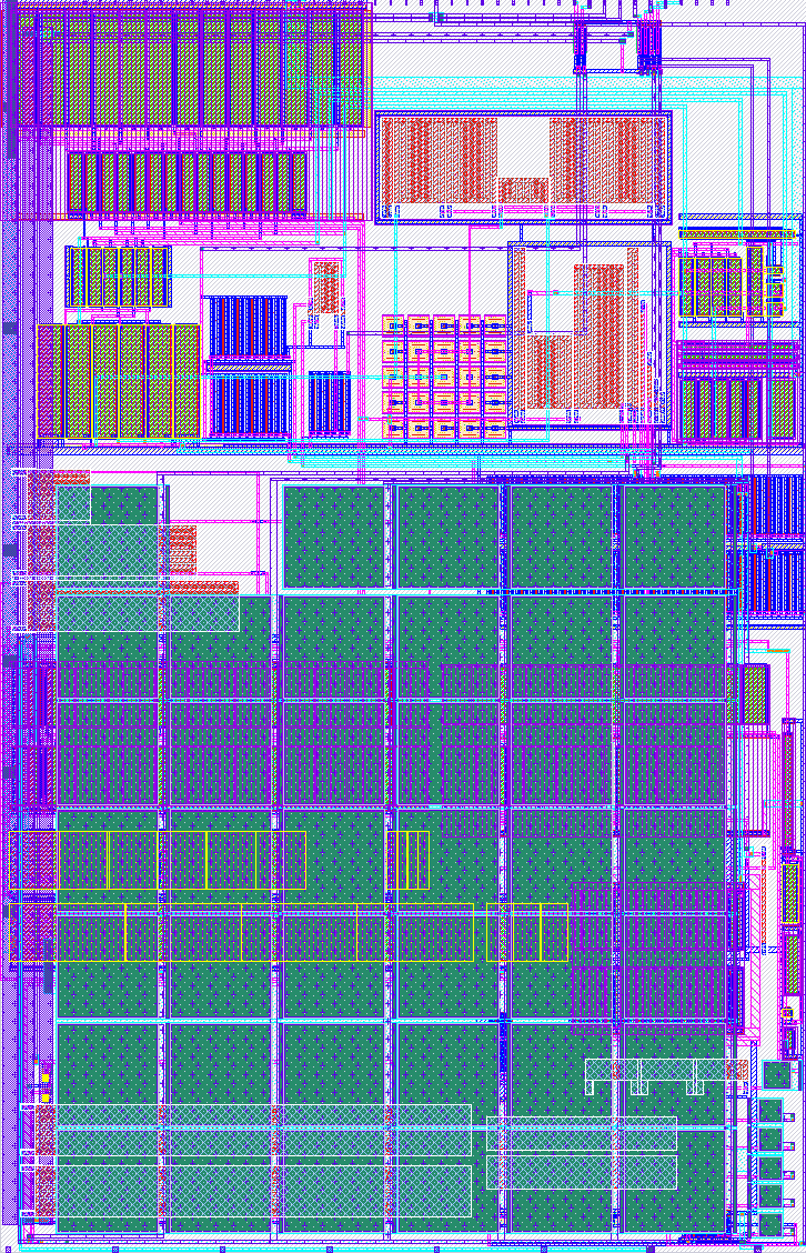
- Author: wecallemjazzyfact
- Description: Banba Current-Mode BGR (1.2V) and Folded-Cascode LDO (1.8V output) for Sky130
- GitHub repository
- Open in 3D viewer
- Open in Tiny Tapeout Explorer
- Clock: 0 Hz
How it works
This design integrates a high-precision Bandgap Reference (BGR) and a high-performance Low-Dropout (LDO) Regulator implemented in the SkyWater Sky130A 130nm CMOS process.
1. Bandgap Reference (BGR)
- Topology: Banba current-mode architecture generating a curvature-compensated reference voltage (~1.20 V).
- Core Components: Vertical PNP substrate BJT pairs ($Q_1, Q_2$), PMOS current mirrors, and matched high-sheet poly resistors.
- Trimming (6-bit): 6-bit binary resistor trim network (
ui_in[7],ui_in[3:0],ui_in[6]) providing a wide 2042.6 mV tuning range with 8.4 mV LSB resolution for post-silicon process and mismatch compensation. - Output: Reference voltage is monitored via analog pin
ua[1](VREF_LOW).
2. Low-Dropout Regulator (LDO)
- Input Supply: 3.3 V high-voltage analog rail (
VAPWR). - Regulated Output: 1.8 V target output on analog pin
ua[0](VDDC, sensing output). - Error Amplifier (EA): Folded-Cascode topology powered directly from
VAPWR(3.3 V) for rail-to-rail control and high gate drive margin. - Pass Transistor: Sized PMOS power device optimized for low dropout voltage and wide load current range.
- Diagnostics: Integrated ring oscillator and frequency divider core for on-chip activity monitoring via digital output
uo[0].
Performance Summary (Post-Layout PEX R+C Verified)
| Parameter | Specification / Conditions | Typical / Measured | Unit |
|---|---|---|---|
| Input Supply Voltage ($V_{APWR}$) | Analog 3.3V power rail | 3.3 | V |
| Digital Supply Voltage ($V_{DPWR}$) | Digital 1.8V power rail | 1.8 | V |
| Target Output Voltage ($V_{DDC}$) | Regulated output (code 28 nominal) | 1.8001 | V |
| Reference Voltage ($V_{REF_LOW}$) | Bandgap core output (code 28 nominal) | 1.2052 | V |
| Monte Carlo Dispersion ($3\sigma$) | Mismatch-only, Stage 3 (LUT rank trim) | 10.251 (Spec: $\pm 36.0$) | mV |
| Monte Carlo Yield | Target window $\pm 36.0\text{ mV}$ ($\pm 2%$) | 100.00 | % |
| Loop Stability (PM / GM) | Middlebrook dual injection (worst-case) | 69.52° / 11.49 dB | deg / dB |
| PSRR (DC / 100 kHz / 1 MHz) | $V_{APWR}$ ripple rejection | −56.5 / −27.7 / −9.2 | dB |
| Load Transient (1 µs) | On-chip sink step (SNK_EN: 0 $\rightarrow$ 1) | −55.4 / +28.8 | mV |
| Line Transient (10 µs) | $V_{APWR}$ 3.0V $\leftrightarrow$ 3.6V step | −2.49 / +1.95 | mV |
| Temperature Drift (tt, −40 to 85°C) | 125°C temperature span | 1.701 (7.56 ppm/°C) | mV |
| Corner Drift (ss, ff, sf) | −40°C to 85°C | 1.87 ~ 2.47 (8.3 ~ 11.0 ppm/°C) | mV |
Corner Drift (fs corner) |
Fast PMOS / Slow NMOS corner | 4.964 (22.03 ppm/°C) | mV |
| VGND On-Chip IR Drop | Max load current condition | 21.3 | mV |
Note on
fsCorner TC: Thefscorner exhibits a higher temperature coefficient ($22\text{ ppm/°C}$) primarily at −40°C due to NMOS/PMOS asymmetry. Even with this variation, the total output voltage stays well within the $\pm 36\text{ mV}$ target budget ($1.8013\text{ V} \sim 1.8063\text{ V}$).
6-bit Trim & Calibration Procedure (★ LUT Rank Required)
Because TRIM5 (18,198 $\Omega$) slightly exceeds the sum of the lower 5 bits (17,886 $\Omega$) by 312 $\Omega$, the raw binary code sequence contains a non-monotonic step between code 31 and code 32 (+9.18 mV overlap). For optimal post-silicon calibration, always apply trim codes in order of voltage-sorted LUT rank (ldo/lut6.txt).
Calibration Algorithm
- Measure initial $V_{DDC}$ at default code 28 ($V_{nominal} \approx 1.800\text{ V}$).
- Calculate target rank adjustment: $\text{rank}{new} = \text{rank}{current} + \text{round}\left(\frac{V_{DDC} - 1.800\text{ V}}{8.377\text{ mV}}\right)$
- Program corresponding 6-bit trim code to external pins: $\text{VTRIM}[5:0] = 63 - \text{code}$ (Note: Input inverters invert the external pin state before the internal pass gates).
Representative LUT Trim Codes (Selection Table)
| Rank | Internal Code | Binary Code (b5..b0) |
External ui_in Pattern |
$V_{DDC}$ [V] | $V_{REF_LOW}$ [V] |
|---|---|---|---|---|---|
| 1 | 00 | 000000 |
111111 |
2.043118 | 1.367783 |
| 10 | 09 | 001001 |
110110 |
1.964961 | 1.315461 |
| 20 | 19 | 010011 |
101100 |
1.879078 | 1.257963 |
| 27 | 26 | 011010 |
100101 |
1.818415 | 1.217355 |
| 28 | 27 | 011011 |
100100 |
1.809592 | 1.211486 |
| 29 | ★ 28 (Target) | 011100 |
100011 |
1.800143 | 1.205153 |
| 30 | 29 | 011101 |
100010 |
1.791420 | 1.199283 |
| 31 | 32 | 100000 |
011111 |
1.783678 | 1.194100 |
| 32 | 30 | 011110 |
100001 |
1.783265 | 1.193824 |
| 33 | 33 | 100001 |
011110 |
1.774872 | 1.188243 |
| 34 | 31 | 011111 |
100000 |
1.774496 | 1.187953 |
| 40 | 37 | 100101 |
011010 |
1.739894 | 1.164788 |
| 50 | 47 | 101111 |
010000 |
1.653406 | 1.106887 |
| 63 | 62 | 111110 |
000001 |
1.523760 | 1.020092 |
How to test
Required Supplies & Power Up Sequence
- Connect
VGNDto Ground (0 V). - Apply
VAPWR= 3.3 V (Analog 3.3 V power rail). - Apply
VDPWR= 1.8 V (Digital 1.8 V power rail).
Pin Mapping & Operation
| Pin | Direction | Signal | Function | Note |
|---|---|---|---|---|
ua[0] |
Analog Out | VDDC |
Regulated 1.8 V LDO Output | Sensing only (on-chip pass device) |
ua[1] |
Analog Out | VREF_LOW |
1.20 V Bandgap Reference Output | Reference monitoring |
ui[0] |
Digital In | trim[1] |
BGR Trim Bit 1 | Internal code bit 1 |
ui[1] |
Digital In | trim[2] |
BGR Trim Bit 2 | Internal code bit 2 |
ui[2] |
Digital In | trim[3] |
BGR Trim Bit 3 | Internal code bit 3 |
ui[3] |
Digital In | trim[4] |
BGR Trim Bit 4 | Internal code bit 4 |
ui[4] |
Digital In | snk_en |
Current Sink Load Enable | Active High (connects on-chip load) |
ui[5] |
Digital In | ro_en |
Ring Oscillator Test Enable | Active High |
ui[6] |
Digital In | trim[5] |
BGR Trim Bit 5 (MSB) | Internal code bit 5 |
ui[7] |
Digital In | trim[0] |
BGR Trim Bit 0 (LSB) | Internal code bit 0 |
uo[0] |
Digital Out | div_out |
Divided RO Clock Output | Divide-by-16 diagnostic clock |
Measurement Steps
- Measure
ua[1](VREF_LOW) using a high-impedance DMM (nominally ~1.205 V at code 28). - Measure
ua[0](VDDC) with a DMM or oscilloscope. Verify output voltage stabilizes at 1.800 V. - Configure
ui_inaccording to the LUT Trim Table to verify trim steps and tuning range. - Set
ui[4]= 1 (snk_en) to engage on-chip sink load (~1.5 mA) and observe load regulation. - Set
ui[5]= 1 (ro_en) to enable the diagnostic ring oscillator; measure the output frequency onuo[0](div_out).
IO
| # | Input | Output | Bidirectional |
|---|---|---|---|
| 0 | trim[1] | div_out | |
| 1 | trim[2] | ||
| 2 | trim[3] | ||
| 3 | trim[4] | ||
| 4 | snk_en | ||
| 5 | ro_en | ||
| 6 | trim[5] (MSB) | ||
| 7 | trim[0] (LSB) |
Analog pins
ua | PCB Pin | Internal index | Description |
|---|---|---|---|
| 0 | K | 5 | VDDC (LDO 1.8V output, sensing only) |
| 1 | C | 0 | VREF_LOW (bandgap 1.2V reference) |