526 CTW LDO and Dynamic Comparator
526 : CTW LDO and Dynamic Comparator
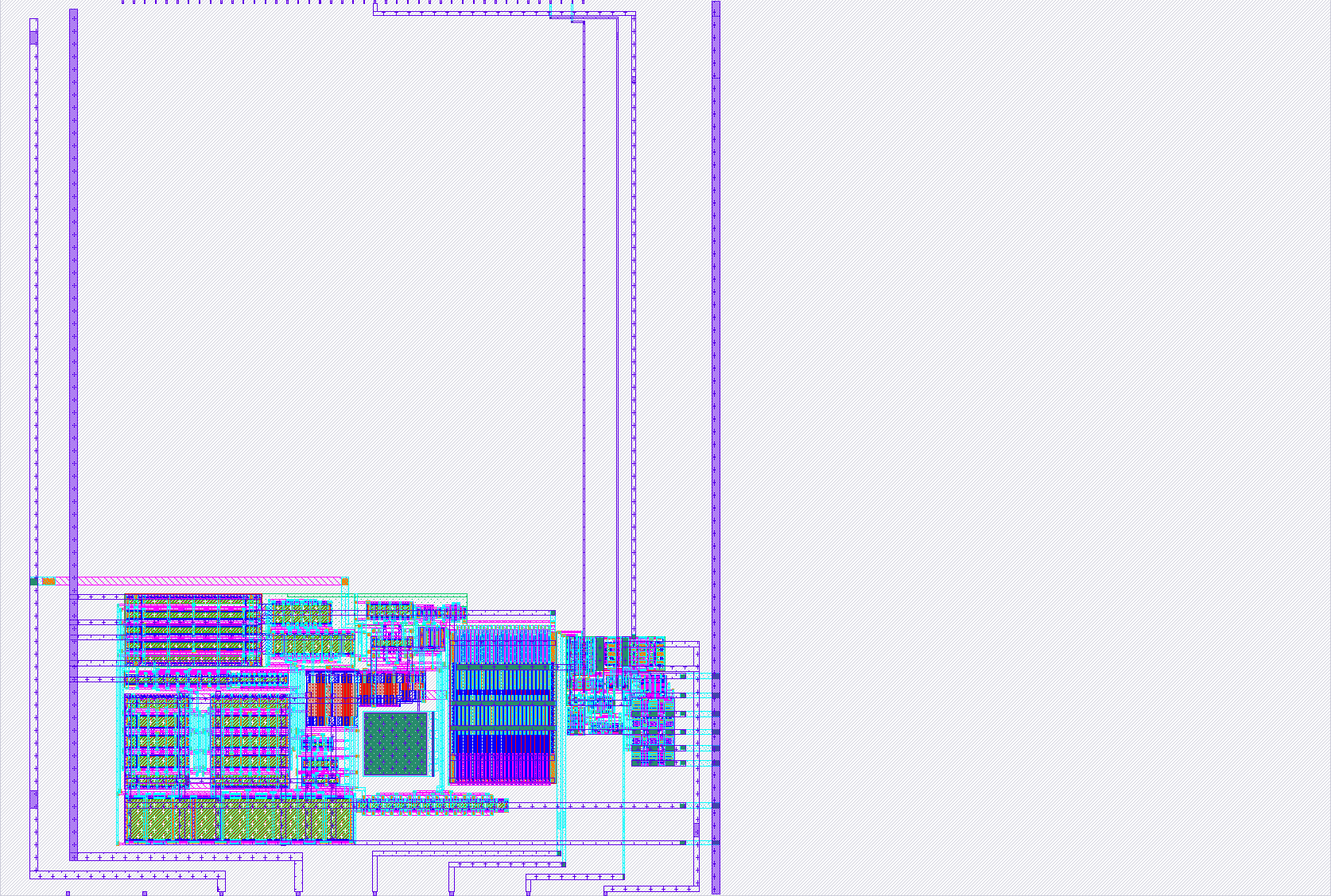
- Author: TuanKiet
- Description: Analog LDO and dynamic comparator test chip in SKY130
- GitHub repository
- Open in 3D viewer
- Open in Tiny Tapeout Explorer
- Clock: 0 Hz
How it works
CTW LDO and Dynamic Comparator is a SKY130 custom analog test chip containing an LDO voltage regulator and a clocked dynamic comparator. The physical top-cell name is tt_um_SAR_ADC; this retained identifier does not imply a complete SAR ADC implementation. The design occupies 2x2 Tiny Tapeout tiles and declares six analog connections.
The LDO regulates an analog output using an external reference connection. The supplied LDO Ver3 pre-layout workbook shows an output near 1.0 V. The comparator evaluates differential analog inputs under the CLKB signal. Its two output connections are exposed for characterization. The Verilog file is an interface declaration; circuit behavior is implemented by the custom layout.
Pin connections
The following functional labels are retained from the supplied layout metadata. Their electrical connectivity has not been independently verified by extracted-netlist comparison.
| Tiny Tapeout connection | Label | Intended role |
|---|---|---|
| ui[0] | CLKB | Comparator clock/control input |
| uo[0] | OUT+ | Comparator output |
| ua[0] | OUT_LDO | LDO output |
| ua[1] | OUT- | Complementary comparator output |
| ua[2] | VIN+ | Comparator differential input |
| ua[3] | VIN- | Comparator differential input |
| ua[4] | VDD | Analog supply connection; confirm routing before powering |
| ua[5] | VREF | External LDO reference |
| VDPWR | VDPWR | Platform power connection |
| VGND | VGND | Ground connection |
Other digital pins have no application function declared in the project metadata. Do not use ua[6] or ua[7]. The internal relationship between ua[4], VDPWR, and the two blocks' supply rails must be confirmed from the schematic or extracted netlist. Do not assume these supplies are interchangeable or that the LDO internally powers the comparator.
Preliminary LDO characterization
Source: SKY130_LDO_Ver3_PRE.xlsx, extracted from the user-supplied RAR archive. These are pre-layout simulation results, not measured silicon specifications. The load-sweep supply is inferred as 1.2 V from the workbook's Vout and Vin-minus-Vout columns.
| Parameter | Conditions | Result |
|---|---|---|
| No-load output | TT, 27 C, Vin = 1.2 V | 1.00392632 V |
| Output at 10 mA | TT, 27 C, load sweep | 0.998309785 V |
| Output change | TT, 27 C, 0 to 10 mA | 5.616535 mV decrease |
| Average load regulation | Same endpoints | 0.5616535 mV/mA |
| Ground current, no load | TT, 27 C | 38.59974 uA |
| Ground current, 10 mA | TT, 27 C | 43.32819 uA |
| No-load line regulation | TT, 27 C, Vin = 1.2 to 1.5 V | 4.55927 mV/V |
| Max-load line regulation | TT, 27 C, Vin = 1.2 to 1.5 V, workbook Max Load table | 4.02168 mV/V |
The workbook includes TT, SS, SF, FS and FF process groups and temperature data at -40, 27 and 90 C. Some headers repeat SS 90 within the SF group; these labels require confirmation before publishing corner-specific limits. Columns named dropout calculate Vin minus Vout and do not establish the minimum input headroom required to maintain regulation.
Preliminary comparator characterization
Source: Comparator_Scientific_Characterization.xlsx, PVT_All_Data and IRN_Offset sheets. The supplied workbook does not establish whether these comparator results include extracted parasitics.
| Parameter | TT, VDD = 1.0 V, 27 C | Range of available PVT results |
|---|---|---|
| Decision time | 3.78 ns | 1.84 to 9.51 ns |
| Reset time | 4.29 ns | 2.90 to 6.98 ns |
| Power | 108.841 uW | 42.600 to 320.671 uW |
The PVT table covers five process corners, VDD = 0.95, 1.00 and 1.10 V, and temperatures of 0, 27 and 125 C. Decision-time results are missing for SF and SS at 0.95 V and 0 C. Reported ranges exclude missing values and are not guaranteed operating limits.
The transient-noise CDF fit reports input-referred noise of 222.32 uVrms with 2.39 uV fit uncertainty, and offset of 0.093 uV with 1.690 uV fit uncertainty (1 sigma). Fit uncertainty is not device mismatch variation. The workbook's maximum-frequency estimate uses twice the decision time and does not account for longer reset times at some corners. Frequency and energy-per-decision limits are therefore not specified here.
How to test
- Before powering the chip, confirm the supply routing, required VREF, permissible input common-mode range, CLKB polarity, clock levels, and output loading from the circuit schematic or extracted netlist. These details are not fully specified by the supplied characterization tables.
- Select the project using the Tiny Tapeout test platform and connect the verified supply and reference sources with a common ground. Use current-limited laboratory supplies. The LDO and comparator workbook voltages describe their respective simulation conditions, not a board-level wiring instruction.
- Measure OUT_LDO with a high-impedance instrument. Start at no load, then apply controlled load steps within the characterized range up to 10 mA. Record output voltage and supply/ground current for comparison with the pre-layout data.
- Sweep the verified LDO input supply while holding reference voltage and load fixed. Compute line regulation as output-voltage change divided by input-voltage change. Test dropout separately using an explicit regulation-error criterion.
- For comparator testing, drive VIN+ and VIN- around a verified common-mode voltage and apply CLKB with adequate evaluation and reset intervals. Probe OUT+ and OUT- with low-capacitance instruments. Confirm output polarity experimentally before interpreting binary results.
- Measure decision and reset times using documented voltage thresholds, input overdrive, clock edge rates, and output capacitance. Begin with a slow clock and increase frequency only after both phases settle reliably.
- Record bench conditions and distinguish simulation results from silicon measurements. Do not treat successful GDS precheck or viewer rendering as electrical validation.
External hardware
- Compatible Tiny Tapeout test platform with access to the allocated analog pins.
- Current-limited supplies for the verified power domains.
- Low-noise adjustable reference source.
- Programmable load or suitable resistor loads for the LDO.
- Differential input source and clock/pattern generator for the comparator.
- DMM and oscilloscope with appropriate low-capacitance probes.
- Decoupling and output capacitors selected according to the verified circuit testbench; capacitor values have not been established by this document.
IO
| # | Input | Output | Bidirectional |
|---|---|---|---|
| 0 | CLKB | OUT+ | |
| 1 | |||
| 2 | |||
| 3 | |||
| 4 | |||
| 5 | |||
| 6 | |||
| 7 |
Analog pins
ua | PCB Pin | Internal index | Description |
|---|---|---|---|
| 0 | Q | 11 | OUT_LDO |
| 1 | X | 6 | OUT- |
| 2 | R | 10 | VIN+ |
| 3 | W | 7 | VIN- |
| 4 | T | 9 | VDD |
| 5 | U | 8 | VREF |