494 NS SAR ADC
494 : NS SAR ADC
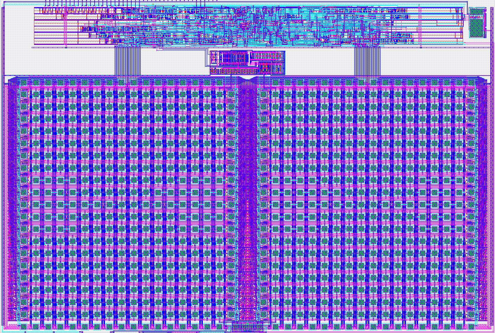
- Author: Silicon Edge
- Description: This is a research project designing a noise shaping SAR ADC design
- GitHub repository
- Open in 3D viewer
- Open in Tiny Tapeout Explorer
- Clock: 0 Hz
How it works
This is an 8-bit differential Successive Approximation Register (SAR) ADC intended to serve as the SAR core of a Noise-Shaping SAR (NS-SAR) ADC.
The ADC uses a differential capacitive DAC (CDAC), a dynamic comparator, and a dedicated digital SAR controller. The differential architecture provides direct conversion of the difference between the two input signals while allowing the common-mode voltage to be independently defined.
The conversion is performed using a charge-redistribution CDAC and successive-approximation algorithm. The CDAC uses bottom-plate switching with dedicated common-mode switching. A common-mode voltage of 0.9 V is used, with a differential reference range defined by VREF_P = 1.8 V and VREF_N = 0 V.
The SAR controller was deliberately designed with the timing sequence of the intended NS-SAR architecture in mind. The controller provides the required phases for sampling, comparator operation and successive approximation, while allowing additional phases required by the future noise-shaping loop to be incorporated. The fabricated implementation requires 12 clock cycles for each conversion, resulting in an 8 kS/s output rate from the 96 kHz input clock.
The CDAC architecture was also designed with Dynamic Element Matching (DEM) in mind. However, DEM is not enabled in the fabricated version. This was an intentional design choice to first verify the fundamental SAR conversion path independently of the additional DEM and noise-shaping circuitry.
The present chip therefore implements the fundamental 8-bit SAR conversion core. The noise-shaping loop and DEM circuitry are reserved for the subsequent NS-SAR implementation, with physical area also allocated to facilitate their future integration.
Design specifications
- Architecture: Fully Differential Conventional Switching SAR
- Resolution: 8 bits
- Input: Differential
- Conversion clock: 96 kHz
- Conversion cycles: 12 clock cycles/conversion
- Output data rate: 8 kS/s
- Positive reference: 1.8 V
- Negative reference: 0 V
- Common-mode voltage: 0.9 V
- Target DNL: ±0.5 LSB
- Target INL: ±1 LSB
- Bias current: 5 µA
- CDAC: Capacitive charge-redistribution DAC
- DEM: Designed for future integration, not enabled
- Noise shaping: Not included in fabricated version
- Intended architecture: Core SAR stage of an NS-SAR ADC
How to test
Connect the differential analog inputs V_P and V_N within the
specified input range. Connect VREF_P to 1.8 V and VREF_N to 0 V.
VCM should be connected to 0.9 V.
A 5 µA bias current should be provided to IBIAS. Apply a 96 kHz clock
to CLK. The RST_N input is active-low and should be tied high for
normal operation. Set EN high to enable the ADC.
Each conversion takes 12 clock cycles. The resulting 8-bit conversion
code is available on uo_out[7:0]. uio_out[0] provides the End of
Conversion (EOC) indicator.
Pinout
| Pin | Signal | Description |
|---|---|---|
ua[0] |
V_N |
Differential negative input(0-1.8V) |
ua[1] |
V_P |
Differential positive input(0-1.8V) |
ua[2] |
VCM |
Common-mode voltage (0.9 V) |
ua[3] |
VREF_P |
Positive reference voltage (1.8 V) |
ua[4] |
VREF_N |
Negative reference voltage (0 V) |
ua[5] |
IBIAS |
Bias current input (5 µA) |
ui_in[0] |
CLK |
Conversion clock (96 kHz) |
ui_in[1] |
RST_N |
Active-low reset |
ui_in[2] |
EN |
Active-high enable |
uo_out[7:0] |
ADC_OUT |
8-bit digital conversion result |
uio_out[0] |
EOC |
End of Conversion indicator |
External hardware
No external hardware is required apart from the clock source, reference voltage sources, and the 5 µA bias current source.
IO
| # | Input | Output | Bidirectional |
|---|---|---|---|
| 0 | B0 | ||
| 1 | B1 | ||
| 2 | B2 | ||
| 3 | B3 | ||
| 4 | B4 | ||
| 5 | B5 | ||
| 6 | B6 | ||
| 7 | B7 |
Analog pins
ua | PCB Pin | Internal index | Description |
|---|---|---|---|
| 0 | K | 5 | VCM |
| 1 | C | 0 | VIN |
| 2 | J | 4 | VIP |
| 3 | D | 1 | VREF_P |
| 4 | G | 3 | VREF_N |
| 5 | F | 2 | IBIAS |