Draw a capacitor
Aim
- Understand that capacitance changes with area and distance
- Investigate capacitance between objects on the same layer
- Creating capacitors using the mimcap layer
- Learn how to get the most capacitance
- Check your design using the DRC
We’ve already seen an example of parasitic capacitance - now let’s intentionally draw a capacitor and see how big of a value we can create.
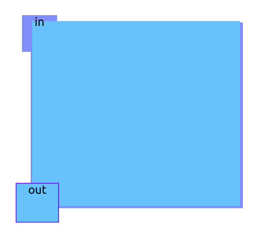
As mentioned, a capacitor is formed whenever we have 2 conductive shapes separated by a non conductive space. Let’s try drawing a capacitor with the metal2 layer.

Use the SPICE checkbox to see the capacitance. You’re looking for a line that looks like C0 out in and then some numbers. I got 0.73fF. The F stands for Farads, the unit of capacitance. The f stands for femto, there are 1,000,000,000,000,000 femto Farads in one Farad! So this is a very tiny capacitor!
Have a go at making a bigger value of capacitor. With resistors, a long thin wiggly shape makes a big resistance. With a capacitor, we want the most area. The biggest I managed using only metal2 was 14fF.
Using more than 1 layer
Now let’s try using 2 layers, metal1 and metal2. Do you think we’ll be able to make a bigger capacitor?
I thought my capacitor would be bigger, but I only managed 0.22fF. The reason this capacitor isn’t as big as the one on metal2 is that the distance between metal1 and metal2 is large compared to the gap we can create on one layer. This can be seen if you look at the equation for the capacitance of two parallel plates:

Where C is the capacitance, ε is the dielectric constant, A is the overlapping area between your layers, and d is the distance between the layers. When the distance d between layers increases, the capacitance decreases.
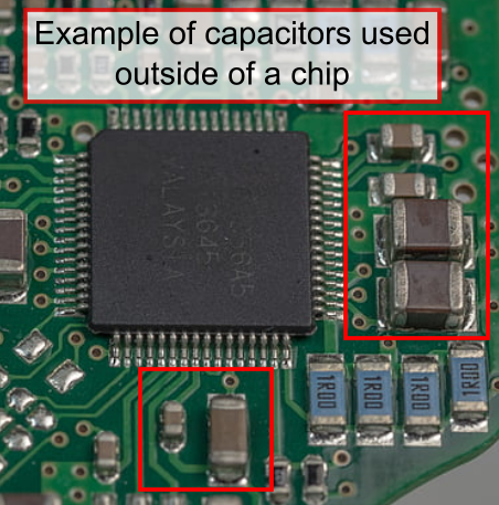
Chips don’t have a lot of area, so making big capacitors on a chip is hard. That’s why we often need to use capacitors outside of the chip if we want really big ones.
However, we do have a way to make better capacitors, and that’s using the mimcap layer. mim stands for “metal insulator metal,” and it’s a special metal layer that’s much closer to metal1 than metal2 is.

Because we can only put labels on metal1 and metal2 layers, we also need a metal2 via to connect the metal2 layer to the mimcap layer.
Run DRC
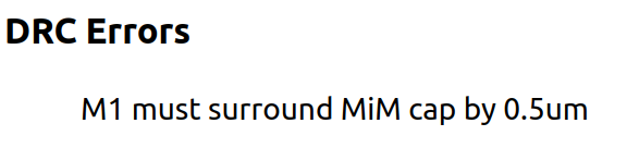
Draw a square of metal1 and on top of that a square of mimcap. Take a look at the DRC report (below the cross section):
DRC stands for Design Rule Check. We can’t just draw whatever we want and have it made into a chip. A big part of the PDK includes DRC rules that make sure we only send designs to the factory that they can actually make.
If you click on the error it will highlight the problem on the canvas. Select metal1 again and draw a bigger square so it extends a little on all sides of the mimcap layer. The error should disappear when it’s resolved.
Maximum capacitance
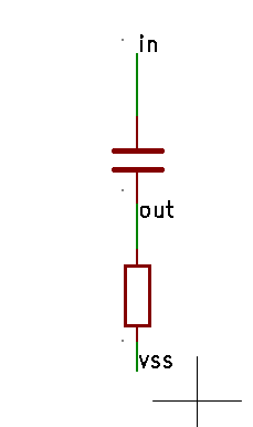
Now that we have a capacitor between the mimcap and metal1 layers, let’s connect up the input and output ports. For the out, you can just add a label to the metal1 layer. To connect a port to the mimcap layer, you’ll need to first use metal2 via and then metal2 above that. Once you’ve drawn the metal2 square, label it as in.


Using the SPICE checkbox, find out your new capacitance. I managed 970fF with the one above, so nearly 5000 times bigger than the one between metal1 and metal2.
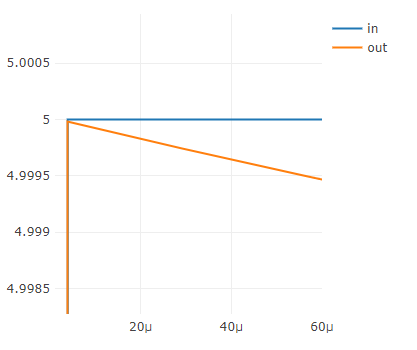
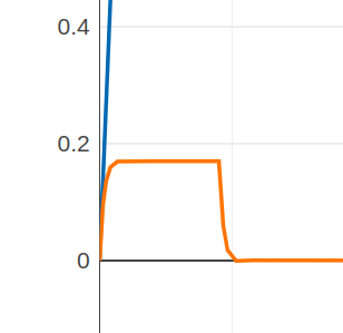
What happens to the output curve when you make the input rise faster by decreasing the rise time?
Now the capacitor is so much bigger than the parasitic one we made when experimenting with the resistor in lesson 1, the output falls much slower. So slow we can’t really see it unless you zoom into the graph a lot.
Pull down
By connecting a pull down resistor between the capacitor and vss we can drain it faster.
If you don’t remember how we made a resistor, go back and take a look. Then follow these steps and see if you can draw it yourself.
- Draw a square of metal1 via so it connects to the metal1 output square
- Draw a long skinny resistor using polyres - maybe make it about 0.5μm thick and 20μm long.
- Use another metal1 via at the end of the resistor
- Draw a square of metal1 above the metal1 via
- Label the metal1 square vss.

You should now see the output voltage doing something different. If we zoom in a bit we can see it more clearly.
If you get stuck, here’s my solution.
Experiment with the input rise time, what happens to the output pulse?
A common use for a combination of a resistor and a capacitor is making a filter. We can filter out some frequencies of inputs and leave others.
As it takes a specific amount of time to charge up and discharge, this circuit can also be used to build a timer.