265 Dual-Path Noise-Shaping ADC
265 : Dual-Path Noise-Shaping ADC
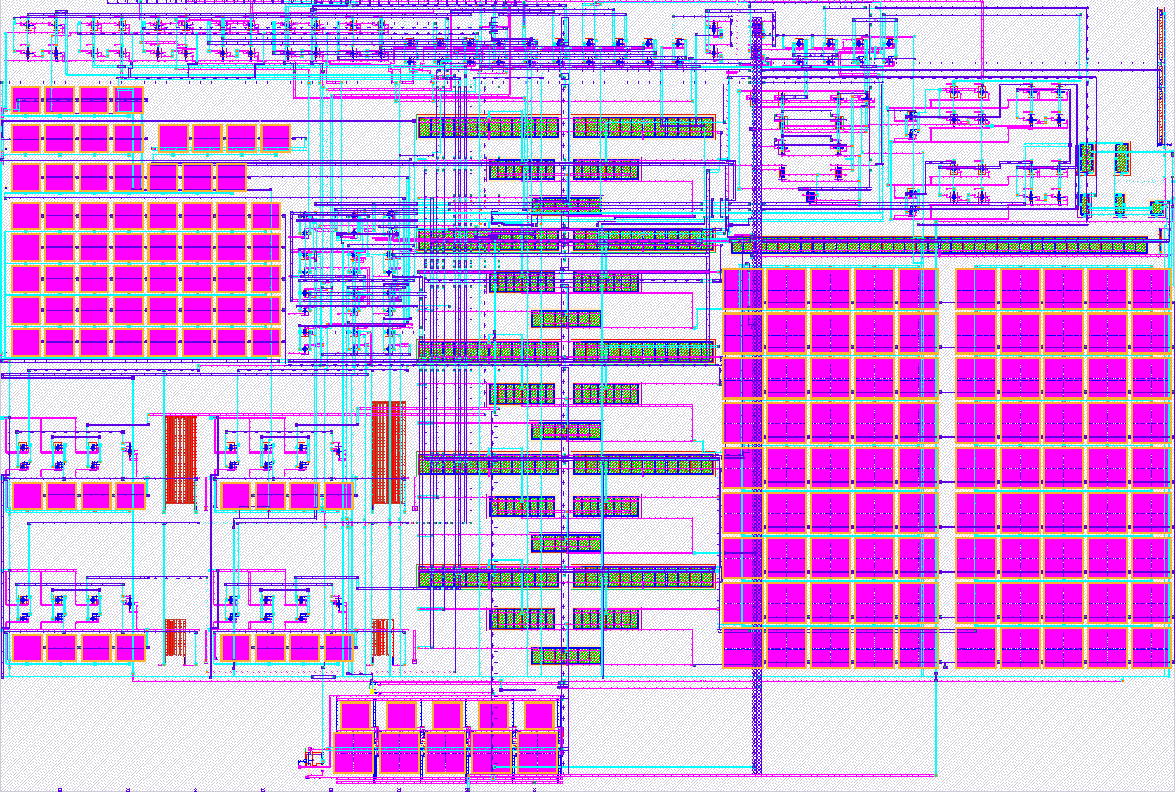
- Author: Tyler McClure
- Description: Two ADC architectures share one analog input: a VCO pulse-frequency path and a first-order switched-capacitor delta-sigma bitstream, with a buffered analog loop monitor.
- GitHub repository
- Open in 3D viewer
- Open in Tiny Tapeout Explorer
- Clock: 500000 Hz
How it works
This project places two independent first-order noise-shaping ADC architectures
on one SKY130 die. Both observe the same single-ended analog input, ua[0], so
their outputs can be compared under the same stimulus:
uo_out[0]is the pulse train from a voltage-controlled oscillator (VCO). An off-chip counter and per-die calibration convert frequency to voltage.uo_out[1]is the raw one-bit stream from a switched-capacitor delta-sigma modulator. Off-chip filtering and decimation produce samples.ua[1]is a buffered analog monitor of the delta-sigma loop state. The storage node itself is not connected directly to the pad.
The design uses the 1.8 V VDPWR supply, occupies a Tiny Tapeout 2x2 analog
tile, and uses two analog pads. It does not use VAPWR or Metal5.
Architecture
                                  +--------------------------+
                                  | five-stage current-      |
ua[0] shared analog input --------+ starved ring oscillator  +--> buffer --> uo_out[0]
        |                         +--------------------------+               pulse train
        |
        |   +-----------------+   +------------------+   +------------------+
        +-->+ input sampling  +-->+ switched-cap OTA +-->+ StrongARM and    +--> uo_out[1]
            | gate and Cin    |   | integrator       |   | held-decision    |    bitstream
            +-----------------+   | with Cf and Cdac |   | latch            |
                                  +--------+---------+   +------------------+
                                           |
                                           +--> high-Z buffer --> ua[1]

clk --> non-overlap/sample/integrate/evaluate timing
rst_n --> loop reset and deterministic restart
VDPWR/VGND --> supply-tracking VINC/VCM references and 0/1.8 V feedback DAC
VCO path
ua[0] controls the starvation devices of a five-stage ring oscillator. A
two-stage output buffer isolates the ring and drives uo_out[0]. The VCO is
asynchronous and free-running; clk and rst_n apply only to the delta-sigma
path. Frequency is intentionally decoded off-chip so each die can be
calibrated for process, temperature, and supply variation.
Delta-sigma path
The first-order modulator uses physical transmission gates and explicit M1/M2
VPP capacitor arrays. The selected arrays are Cin=0.256550 pF,
Cf=1.466000 pF, and Cdac=0.146600 pF (7:40:4 units). Their final-route TT
one-cycle coefficients are approximately 0.17302 for the input and 0.09762 for
the feedback DAC.
During the sample/evaluate portion of a cycle, the input and DAC capacitors
sample their references while the StrongARM comparator updates a static held
decision latch. During integration, charge is transferred into Cf; the
previously held decision selects either VGND or VDPWR for negative feedback.
On-chip non-overlap logic derives every phase from the external 500 kHz clk.
A buffered 11:1:12 supply-tracking ladder generates nominal
VCM=0.900 V and VINC=0.975 V. The integrator monitor reaches ua[1] only
through a high-input-impedance buffer.
Pin interface
| Pin | Direction | Function |
|---|---|---|
ua[0] |
analog input | Shared ADC input, characterized from 0.750 to 1.200 V |
ua[1] |
analog output | Buffered delta-sigma loop-state monitor |
uo_out[0] |
digital output | Raw VCO pulse train |
uo_out[1] |
digital output | Raw delta-sigma one-bit stream |
clk |
digital input | 500 kHz, 50% duty delta-sigma sample clock |
rst_n |
digital input | Active-low delta-sigma reset |
VDPWR |
power | Nominal 1.8 V supply |
VGND |
power | Ground |
ena, ui_in, and uio_in are unused by the project circuit. All unused
uo_out, uio_out, and uio_oe bits are physically tied to VGND. Unused
analog pads remain isolated.
Characterized operating point
| Quantity | Value |
|---|---|
| Supply | 1.80 V nominal |
| Shared input range | 0.750--1.200 V |
| Input/reference center | 0.975 V |
| Internal common mode | 0.900 V nominal |
| Delta-sigma clock | 500 kHz, 50% duty |
| Feedback DAC levels | 0 V / 1.8 V |
| Shaping test target | 8,192 output bits, OSR 128, 1220.703125 Hz tone |
The input range is an absolute single-ended voltage range, not a differential
common-mode specification. Keep ua[0] inside this range and use a stable,
low-impedance source. The characterized clock has 50% duty; the available 40%
and 60% controls generally violate phase or timing limits and do not establish
a duty-cycle tolerance. Do not use 1 MHz as an unconditional PVT operating
point: extracted passive-corner checks lose timing margin at HH and suppress
evaluation at SS_HH.
At 500 kHz/50% duty, the extracted clock block passes all 24 legal installed MOS/passive model sections both at their screened supply/temperature defaults and at 1.8 V/27 C. A separate SS_HH check at 1.62 V/125 C passes all 15 combinations of 0.1/1/10 ns clock edges and five reset-release phases. The short final-top SS_HH check produces valid, monotonic decisions at 0.750, 0.975, and 1.200 V. These deterministic simulations establish the bring-up mode; they do not specify statistical yield or a guaranteed clock tolerance.
The tables below collect the production-facing simulation and extracted-layout results used for signoff. Intermediate bring-up sweeps and deliberately broken fault controls are mentioned only where they establish that a check is live; they are not device specifications.
Final extracted dual-top results
The following values come from the final promoted layout and its fresh post-promotion replays, not from the earlier schematic-only model.
| Measurement | Final extracted result |
|---|---|
VCO frequency, DSM quiet / active, at ua[0]=0.975 V |
10.692548 / 10.692438 MHz |
| VCO change while DSM switches | 0.001026% |
| DSM 24-bit coexistence density | 0.500000 |
| DSM continuous state | 0.819201--1.006700 V |
| VCM during coexistence | 0.888687--0.915446 V |
| VINC during coexistence | 0.964113--0.984608 V |
| Buffered monitor with 5 pF load | 0.878370--0.951829 V |
| Quiet / active average supply current | 149.750 / 157.768 uA |
| Peak supply current | 0.995 mA |
| Incremental active-versus-quiet peak current | 659.887 uA |
| Direct extracted VCO/DSM coupling | 20.658780 fF |
| Worst VDPWR / VGND user-route resistance | 153.599790 / 475.701875 ohm |
| Shared post-boundary VCO/DSM VDPWR resistor components | 0 |
The deliberate 1 pF clock-to-ring coupling control is rejected, confirming that the coexistence test is sensitive to excessive cross-domain coupling.
Shared-input loading
Measurement from formal ua[0] |
Result |
|---|---|
| Worst route to any of five VCO control gates | 223.300 ohm |
| Route to the DSM sampling-switch conductor landing | 85.987 ohm |
| Conservative off-state capacitance | 0.093877 pF |
| Conservative on-state capacitance, including the DSM input bound | 0.375728 pF |
These values are comfortably below Tiny Tapeout's 500 ohm and 5 pF analog-path screens. Synthetic open and short controls are both rejected. The reported 752.048 ohm route to the minimum-width DSM PMOS terminal includes 666.061 ohm of local source/drain device access; it is not pad wiring. The switch itself was separately qualified across PVT with 2.020--44.338 kohm on-resistance and passed settling, leakage, and feedthrough limits.
VCO characterization and off-chip conversion
The resistance-aware TT curve of the unchanged VCO core is strictly monotonic over 19 points from 0.750 to 1.200 V. It spans 2.775095--19.775050 MHz, with a 27.196400--41.800400 MHz/V local slope. Its dense-sweep center is 11.495830 MHz; an independent nominal distributed-RC run measured 11.4954 MHz. Earlier capacitance-only corner qualification at 1.000 V measured 9.7012 MHz at SS and 15.4025 MHz at FF, and both corners self-started without hidden initial conditions. The capacitance-only central slope is 43.03 MHz/V.
ua[0] |
TT frequency | Maximum terminal stress |
|---|---|---|
| 0.750 V | 2.775095 MHz | 1.802470 V |
| 0.775 V | 3.455005 MHz | 1.803060 V |
| 0.800 V | 4.196578 MHz | 1.803640 V |
| 0.825 V | 4.991435 MHz | 1.804200 V |
| 0.850 V | 5.831403 MHz | 1.804740 V |
| 0.875 V | 6.709342 MHz | 1.805240 V |
| 0.900 V | 7.619381 MHz | 1.805710 V |
| 0.925 V | 8.556728 MHz | 1.806150 V |
| 0.950 V | 9.517437 MHz | 1.806560 V |
| 0.975 V | 10.498130 MHz | 1.806940 V |
| 1.000 V | 11.495830 MHz | 1.807300 V |
| 1.025 V | 12.507790 MHz | 1.807590 V |
| 1.050 V | 13.531420 MHz | 1.808100 V |
| 1.075 V | 14.564230 MHz | 1.808710 V |
| 1.100 V | 15.603700 MHz | 1.809320 V |
| 1.125 V | 16.647270 MHz | 1.809910 V |
| 1.150 V | 17.692280 MHz | 1.810480 V |
| 1.175 V | 18.735910 MHz | 1.811060 V |
| 1.200 V | 19.775050 MHz | 1.811600 V |
Use rising-edge counts in half-open windows and build a monotonic per-die LUT with training voltages 0.750, 0.800, ..., 1.200 V. Across 1,024 asynchronous window phases, the nominal TT calibration model produced:
| Window | Conversion rate | Effective count span | Median / worst edge-quantization estimate | Worst held-out calibrated error |
|---|---|---|---|---|
| 10 us | 100 ksample/s | 170 | 2.5273 / 3.5175 mV | 3.4863 mV |
| 100 us | 10 ksample/s | 1,700 | 0.2527 / 0.3517 mV | 1.2605 mV |
| 1 ms | 1 ksample/s | 17,000 | 0.0253 / 0.0352 mV | 1.0847 mV |
These calibration errors include counter quantization and curve interpolation; they do not include physical oscillator jitter, board noise, source noise, or silicon mismatch.
Delta-sigma characterization
Selected 500 kHz operating point
At the screened SS_HH passive/process corner, 1.62 V, and 125 C, complete 2,048-bit final-top records are monotonic across the input range:
ua[0] |
Density | Longest run | Continuous state | Solver |
|---|---|---|---|---|
| 0.750 V | 0.360352 | 2 | 0.65553--0.91835 V | second-order Gear |
| 0.975 V | 0.603027 | 2 | 0.68400--0.94734 V | ngspice default |
| 1.200 V | 0.846680 | 6 | 0.70987--0.97309 V | ngspice default |
All retained samples are valid logic values, both decisions occur at every
input, and the continuous loop state stays inside the registered
VDD/2 +/- 0.3 V window. The low-input default-method run stopped in a VPP
model square-root/timestep failure after 1,633 valid samples; the complete
Gear rerun is retained as a numerical control rather than treating ngspice's
zero process status as success.
Eight separate SS_HH/1.62 V/125 C final-top cases pass the registered recovery
and interface limits: baseline startup, a warm reset, clock stop/restart, reset
before clock start, a 50 us supply ramp, delayed input application, explicit
pin loading, and a bounded 5 ohm external supply. The interface case includes
500 ohm/5 pF at ua[0], 1 kohm/0.245 pF at clk, and 50 fF at each digital
output. Every case returns valid logic with both decisions, bounded state and
references, full VCO swing, and less than 0.619 mA simulated peak supply
current. These are deterministic extracted simulations, not package or board
qualification.
A complete selected-point 8,192-bit shaping record is unavailable. The default ngspice transient remained functional for 3,344 retained bits, then stopped in a VPP model square-root/timestep failure. A second-order Gear rerun reached its fixed six-hour timeout without producing a complete stream. No current transistor-level SNDR, ENOB, SFDR, THD, or shaping-slope value is claimed. Use the 500 kHz setting for screened functional bring-up and characterize converter performance on returned silicon before relying on an accuracy or noise figure.
Historical nominal-clock DC transfer and startup
The tables in this subsection are retained nominal-condition results from the earlier 1 MHz characterization. They do not override the 500 kHz/50% duty operating point above or establish 1 MHz operation across PVT.
The final 2,048-bit extracted DC/reset/held-decision gate produced monotonic density at all three input points:
ua[0] |
Extracted density | Behavioral control | Longest identical-bit run | State range |
|---|---|---|---|---|
| 0.750 V | 0.27294922 | 0.28173828 | 3 | 0.73935--0.99859 V |
| 0.975 V | 0.49316406 | 0.50048828 | 2 | 0.75527--1.03026 V |
| 1.200 V | 0.71289062 | 0.71923828 | 3 | 0.77474--1.05513 V |
A reversed-DAC control locks at zero density and is rejected. The complete nine-case TT/SS/FF matrix is monotonic; its worst extracted-versus-control density error is 0.015625, its longest run is six bits, and every state remains inside the registered corner-relative +/-300 mV window:
| Corner | ua[0] |
Extracted density | Behavioral control | Longest run | State range |
|---|---|---|---|---|---|
| TT | 0.750 V | 0.273438 | 0.281250 | 3 | 0.7393--0.9985 V |
| TT | 0.975 V | 0.492188 | 0.500000 | 2 | 0.7559--1.0297 V |
| TT | 1.200 V | 0.710938 | 0.718750 | 3 | 0.7751--1.0545 V |
| SS | 0.750 V | 0.351562 | 0.359375 | 2 | 0.6681--0.9107 V |
| SS | 0.975 V | 0.593750 | 0.609375 | 2 | 0.7180--0.9290 V |
| SS | 1.200 V | 0.843750 | 0.851562 | 6 | 0.7264--0.9653 V |
| FF | 0.750 V | 0.218750 | 0.226562 | 4 | 0.7728--1.0770 V |
| FF | 0.975 V | 0.421875 | 0.429688 | 2 | 0.8046--1.1050 V |
| FF | 1.200 V | 0.617188 | 0.632812 | 2 | 0.8317--1.1262 V |
At the center input, separate short bring-up runs measured density/state of 0.500000 and 0.7659--1.0135 V at TT, 0.593750 and 0.7184--0.9290 V at SS, and 0.437500 and 0.8046--1.1026 V at FF.
The deterministic comparator-offset campaign covers TT/SS/FF, both offset signs, and all three inputs: all 18 cases pass for the allocated +/-40 mV threshold shift:
| Corner | Offset | ua[0] |
Extracted density | Control | State range |
|---|---|---|---|---|---|
| TT | -40 mV | 0.750 V | 0.273438 | 0.289062 | 0.6915--0.9633 V |
| TT | -40 mV | 0.975 V | 0.500000 | 0.500000 | 0.7161--0.9900 V |
| TT | -40 mV | 1.200 V | 0.718750 | 0.718750 | 0.7374--1.0151 V |
| TT | +40 mV | 0.750 V | 0.273438 | 0.281250 | 0.7742--1.0417 V |
| TT | +40 mV | 0.975 V | 0.492188 | 0.500000 | 0.7938--1.0710 V |
| TT | +40 mV | 1.200 V | 0.710938 | 0.718750 | 0.8149--1.0942 V |
| SS | -40 mV | 0.750 V | 0.359375 | 0.359375 | 0.6282--0.9114 V |
| SS | -40 mV | 0.975 V | 0.601562 | 0.601562 | 0.6614--0.8966 V |
| SS | -40 mV | 1.200 V | 0.843750 | 0.843750 | 0.6873--0.9247 V |
| SS | +40 mV | 0.750 V | 0.359375 | 0.367188 | 0.7111--0.9912 V |
| SS | +40 mV | 0.975 V | 0.601562 | 0.609375 | 0.7417--0.9637 V |
| SS | +40 mV | 1.200 V | 0.843750 | 0.851562 | 0.7665--1.0050 V |
| FF | -40 mV | 0.750 V | 0.218750 | 0.226562 | 0.7330--1.0364 V |
| FF | -40 mV | 0.975 V | 0.421875 | 0.429688 | 0.7638--1.0626 V |
| FF | -40 mV | 1.200 V | 0.625000 | 0.625000 | 0.7919--1.0866 V |
| FF | +40 mV | 0.750 V | 0.210938 | 0.226562 | 0.8127--1.1146 V |
| FF | +40 mV | 0.975 V | 0.414062 | 0.421875 | 0.8431--1.1451 V |
| FF | +40 mV | 1.200 V | 0.625000 | 0.632812 | 0.8709--1.1688 V |
This is a deterministic robustness allocation, not a statistical mismatch-yield claim.
Historical nominal-clock noise shaping
The original transistor bitstreams behind this table were not retained. A later audit found that the analysis helper included out-of-band harmonic power in its in-band distortion sum, so the numerical SNDR/ENOB values below are historical and unrecomputed. They are not supported performance claims.
| Extracted 8,192-bit case | Slope | SNDR | ENOB estimate | Continuous state |
|---|---|---|---|---|
| Closed DSM core | 15.410809 dB/dec | 44.335961 dB | 7.072419 bits | 0.72973--1.04582 V |
| Final 1 kohm + 0.245 pF clock load | 16.399652 dB/dec | 43.177696 dB | 6.880016 bits | 0.72933--1.04633 V |
The total modeled clock input capacitance is 0.244664 pF at 1.8 V. A deliberate 10 kohm full-record clock-drive stress fails the shaping criteria, providing a live negative control. The shaping measurements use a converged 2.5 ns maximum transient timestep; a coarser 5 ns run produced a numerical late-lock artifact and is not used as signoff evidence.
Qualified analog blocks
| Block | Simulation summary |
|---|---|
| OTA with physical bias | Nominal gain 43.77 dB, UGF 19.97 MHz, phase margin 58.2 degrees, 20.6/21.5 ns settling; PVT minimum gain 41.87 dB, minimum UGF 11.27 MHz, worst settling 35.55 ns |
| StrongARM comparator | All +/-1 mV and +/-5 mV decisions pass at 0.75/0.90/1.20 V common mode; extracted decision delay 0.288--2.528 ns |
| VINC/VCM references | Unloaded error below 2 mV; switched settling inside 5 mV; PVT ripple 16.6--42.7 mV peak-to-peak; active reference current 69.1--86.9 uA |
| SC integrator | Final-route TT input coefficient 0.173020, DAC coefficient 0.097620/0.097654, null step -1.031 mV, input loading 0.278994 pF |
Physical verification
- Final drawn bounds are 334.86 x 225.76 um inside the 334.88 x 225.76 um Tiny Tapeout 2x2 frame.
- Full Magic DRC is clean, with deliberate bad-geometry controls detected.
- LVS matches uniquely and without property errors at 180 devices and 63 nets per side; missing-diode and wrong-net controls are rejected.
- The interface contains exactly 53 formal ports and 31 unique electrical nets, including 22 intentional grounded output aliases.
- All external functional nets are pairwise isolated.
- The exact antenna audit passes with its deliberate violation control live.
- The hierarchy contains no Metal5.
- Independent builds and normalized GDS/LEF exports are byte-identical; the semantic GDS round trip and Tiny Tapeout precheck pass.
How to test
- Apply 1.8 V to VDPWR and connect VGND. Select/enable the project through the Tiny Tapeout multiplexer.
- Hold
rst_nlow and apply a 500 kHz clock with 50% duty toclk. Keep reset asserted for at least four complete clock cycles, then release it away from a clock transition. The VCO path does not require the clock or reset. - Drive
ua[0]from a stable, low-impedance source between 0.750 and 1.200 V. - Capture rising edges on
uo_out[0]. Calibrate each die with known voltages before converting edge counts to input voltage. - Wait at least 128 complete cycles after reset release, clock restart, or a
material input step. Capture one
uo_out[1]value per clock cycle, preserve the raw stream, and apply an off-chip low-pass/decimation filter. An OSR-128 block average produces 3,906.25 output samples/s. Use raw density as an initial bring-up check. - If needed, observe
ua[1]with a high-impedance instrument. Do not heavily load this diagnostic output.
Suggested equipment is a stable analog source, a 500 kHz clock source, a logic analyzer or FPGA/MCU counter, and a high-impedance oscilloscope or ADC for the monitor pin.
Interpretation and limitations
All numerical results above are simulations or extracted-layout checks, not guaranteed silicon specifications. The VCO requires per-die calibration. Foundry-model mismatch seeds were not sufficiently reproducible to support a yield percentile, and physical VCO jitter/phase noise is deferred to silicon. Consequently no VCO-path SNR, SNDR, THD, or ENOB is claimed here.
The historical delta-sigma SNDR and ENOB values came from one finite extracted simulation record at the stated tone, clock, OSR, and nominal condition. The raw record is unavailable for corrected reanalysis, so those values are not a current performance claim. They also omitted board noise, clock jitter, source distortion, package effects, and statistical mismatch. Characterize both paths on returned silicon before assigning measured performance.
IO
| # | Input | Output | Bidirectional |
|---|---|---|---|
| 0 | VCO-ADC pulse train | ||
| 1 | Delta-sigma bitstream | ||
| 2 | |||
| 3 | |||
| 4 | |||
| 5 | |||
| 6 | |||
| 7 |
Analog pins
ua | PCB Pin | Internal index | Description |
|---|---|---|---|
| 0 | R | 10 | Shared analog input |
| 1 | W | 7 | Buffered delta-sigma loop monitor |