967 Communotron
967 : Communotron
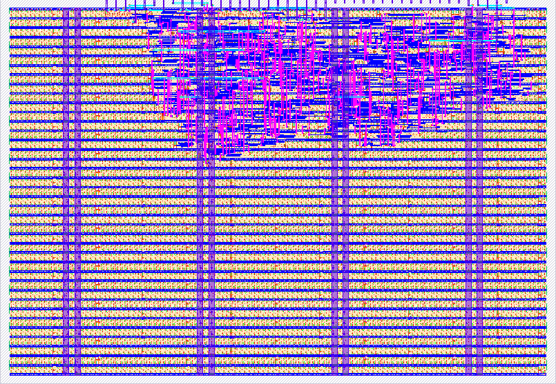
- Author: Garnet Koebel
- Description: A prototype I2C to SPI translator
- GitHub repository
- Open in 3D viewer
- Open in Tiny Tapeout Explorer
- Clock: 400000 Hz
How it works
So you want to communicate?
The Blurb Version
The communotron is a prototype I2C to SPI translator. It only operates in one direction (I2C to SPI). Four pre-programmed addresses are baked into the device 0x41 to 0x44. Sending a I2C message to an address causes the respective chip select pin to activate and the data portion of the I2C message is passed through to the SPI bus. I2C ACK bits are stripped out of the SPI data stream by stalling the clock during each ACK. The device detects I2C stops though this version is finicky on resetting so for more reliable operation it is reccomended to hold reset low for at least two CLK cycles between transmissions. The design was simulated using a 100KHz I2C clock and a 400KHz Chip clock. Seperate pins are used for data input and acking to avoid use of the bi-directional pins.
Frame Handler
The Frame Handler is a finite state machine that detects I2C start, stop, and frame end conditions and generates the driving signals needed to control I2C to SPI translation. The frame_end_oneshot signal is inverted and used to drive the sda_out signal which the Communotron uses to ACK I2C frames.
Match Unit
The Match Unit is a set of four i2c_address_detectors that looks for the pre-programmed addresses during the I2C address frame. The Match Unit's match_x outputs drive the spi_cs_x output pins. After any address is matched an inhibit signal is generated to prevent attempting to select multiple SPI devices in case the data frame(s) contain a valid address.
SPI Clock Stall
Some simple logic uses the frame_end_oneshot signal and scl to stall spi_clk during I2C ACKs stripping these bits from the spi_pico data stream at the cost of slowing down the effective data rate.
But Why?
The use case for a Communotron is primarily a learning experience in ASIC design especially since this iteration is uni-directional. It may be useful for interfacing with chips that only feature SPI communication since the Communotron could be placed closer to said devices thereby saving on PCB area by reducing the length of the SPI bus. It could also be used as rudimentary addressed digital outputs though the overhead of that application is much worse than simply using GPIO.
How to test
- Connect
clkto a 400KHz clock source. - Connect
rst_nto a logic high source - Connect
spi_pico,spi_clk, andspi_cs_1to seperate oscilloscope channels. - Connect
sda_inandsda_outtogether and to a I2C SDA line. - Connect
sclto a I2C SCL line. - Connect a I2C controller (or other device that can generate I2C sequences) to the I2C bus.
- Transmit a I2C Write message to address
0x41. Observe that after the address is transmittedspi_cs_1will go high and the data portion of the message should show onspi_picoless the ACK bits which will be stripped out by means of stallingspi_clk. - Hold
rst_nlow for at least twoclkcycles to reset the Communotron.
External hardware
Possibly external drivers will be needed to safely use this on a I2C bus. No intentionally required external hardware is required.
IO
| # | Input | Output | Bidirectional |
|---|---|---|---|
| 0 | I2C SDA Input (sda_in) | I2C SDA Output (sda_out) | |
| 1 | I2C SCL (scl) | SPI Chip Select 1 (spi_cs_1) | |
| 2 | SPI Chip Select 2 (spi_cs_2) | ||
| 3 | SPI Chip Select 3 (spi_cs_3) | ||
| 4 | SPI Chip Select 4 (spi_cs_4) | ||
| 5 | SPI Peripheral In Controller Out (spi_pico) | ||
| 6 | SPI Clock (spi_clk) | ||
| 7 |