711 Sky TPU 3x3
711 : Sky TPU 3x3
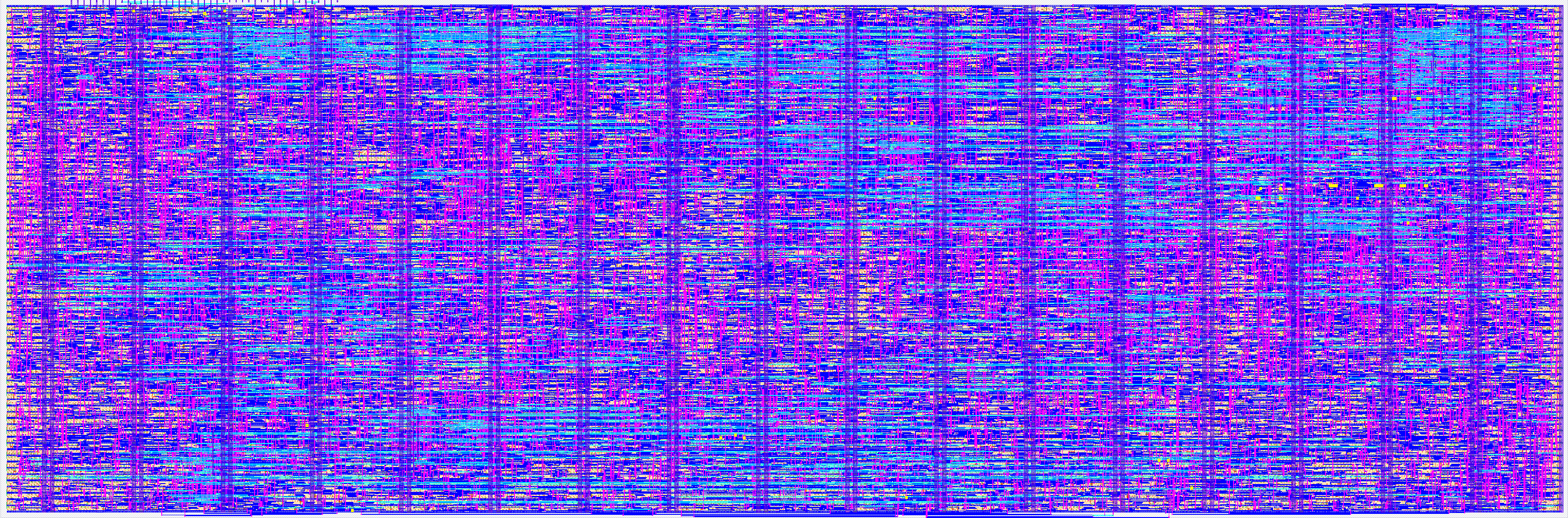
- Author: DashLegion
- Description: int4 systolic-array band-engine TPU: dual-plane 3x3 MACs, 8-deep accumulator, requant+ReLU, autonomous SPI-RAM DMA, on-chip layer chaining
- GitHub repository
- Open in 3D viewer
- Open in Tiny Tapeout Explorer
- Clock: 50000000 Hz
How it works
Sky TPU 3x3 is a complete int4 "band engine" TPU: a 3x3 systolic array of pipelined 4-bit MACs with two weight planes (double-buffered, so the next tile loads while the current one computes), an 8-deep accumulator bank (15-bit saturating, one bank per output column), a requantize + ReLU readout path, and an autonomous SPI-RAM DMA engine.
It computes matrix products in bands: for a band of R output rows (R <= 8), the host streams activation vectors through the array against up to Nb weight tiles; the bank accumulates 3-column partial sums across tiles. Results read out either as int4 (requantized, one 12-bit frame per row) or raw (15-bit accumulator words, 4 frames per row, plus per-column overflow flags).
Everything is driven by an 8-bit beat bus on ui[7:0] (one beat per clock,
0x00 = NOP). Commands: 0x1r+value = CSR write, 0x2_ = LOAD_TILE, 0x3_ =
RUN_PASS, 0x4_ = READ_BAND, 0x5_ = STATUS. In GPIO mode, weights and
activations follow as payload beats. In SPI mode the chip fetches everything
itself from an external SPI RAM: one LOAD_TILE + one RUN_PASS runs the whole
band autonomously (tile prefetch interleaved with compute).
The writeback engine can also stream results back to the SPI RAM. In int4 mode the written format is the activation input format, so one band's output becomes the next band's input: multi-layer neural network inference runs on-chip, with the host sending only command beats. This is verified in simulation with a two-layer chained network.
Output frames appear on {uio[7:4], uo[7:0]} at count-deterministic
offsets from each command header (no valid pin, no polling — the bus reads
0x000 between frames):
| Event | First frame | Cadence |
|---|---|---|
| READ_BAND, int4 mode | header + 6 | one frame per row, every 3 |
| READ_BAND, raw mode | header + 7 | 4 back-to-back frames per row, rows every 4 (row k starts at 7 + 4k) |
| STATUS | header + 3 | single frame |
Guaranteed operation to 83 MHz (12 ns, slow corner, all-corners clean signoff); typical silicon closes at ~116 MHz. The routed netlist was verified pin-exact against the RTL by a cycle-accurate gate-level miter over the full verification campaign.
How to test
Clock the design and drive beats on ui[7:0] synchronously (the RP2040 PIO on
the demo board is ideal: it owns both clock and data). Minimal GPIO-mode
session, 4x3 output, one tile:
- CFG:
0x10 0x03(signed activations + weights),0x12 0x02(shift=2),0x13 0x04(R=4),0x14 0x01(Nb=1) - LOAD_TILE:
0x20then 6 payload bytes — rows bottom-first, each row packed{w_col1, w_col0}then{0, w_col2}(int4 nibbles) - Pad >= 8 NOPs (host contract H2b — the engine is settling the plane)
- RUN_PASS:
0x30then 2R payload bytes — activation rows in the same nibble-pair packing - Wait ~20 clocks for drain, then READ_BAND:
0x40, and sample{uio[7:4], uo}at header+6, +9, +12, +15: each frame is{y2, y1, y0}, requantizedfloor((sum + 2^(shift-1)) / 2^shift)clamped to [-8, 7]. - STATUS (
0x50, frame at +3): bits [2:0] FSM state (0 = idle), [9] = band-done sticky, [6:4] = per-column overflow flags.
For SPI mode, set MODE bit 4, write BASE_A/B/C (CSRs 7/8/9, two bytes LE), and
attach an SPI RAM. test/test.py runs an automated GPIO-mode version of the
above (two-tile accumulation band + STATUS + quiet-bus + offset checks)
against a Python golden model in cocotb.
External hardware
Optional but recommended: a 64 KiB SPI RAM on the uio[3:0] pins (mode 0,
commands 0x03/0x0B/0x02, 16-bit address) — either a PSRAM Pmod or a second
RP2040 running MichaelBell's spi-ram-emu. Without it, GPIO mode provides
full functionality with the host streaming all data. The SPI clock divider
and CS recovery gap are CSR-programmable (CSRs 5 and 6) to accommodate slow
RAM emulation.
IO
| # | Input | Output | Bidirectional |
|---|---|---|---|
| 0 | BEAT0 (command/payload beat bus, NOP=0x00) | FRAME0 (12-bit output frame, count-deterministic offsets) | SPI_CS_N (out, to SPI RAM) |
| 1 | BEAT1 | FRAME1 | SPI_MOSI (out) |
| 2 | BEAT2 | FRAME2 | SPI_MISO (in) |
| 3 | BEAT3 | FRAME3 | SPI_SCK (out) |
| 4 | BEAT4 | FRAME4 | FRAME8 (out) |
| 5 | BEAT5 | FRAME5 | FRAME9 (out) |
| 6 | BEAT6 | FRAME6 | FRAME10 (out) |
| 7 | BEAT7 | FRAME7 | FRAME11 (out) |