233 Azara CiROM ternary read
233 : Azara CiROM ternary read
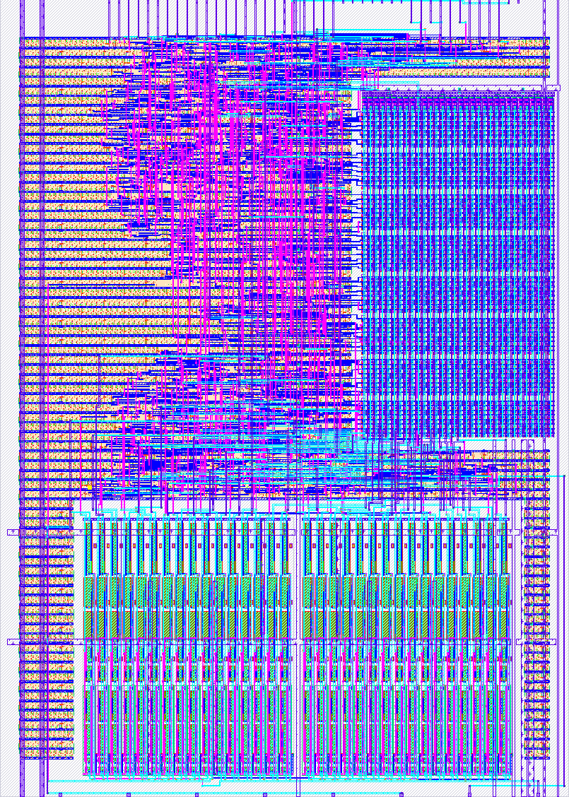
- Author: mpai17
- Description: Mask-programmed ternary compute-in-ROM: single-strobe parallel sense of a 64x32 1T NOR array via single-ended StrongARM amps vs an on-chip VREF
- GitHub repository
- Open in 3D viewer
- Open in Tiny Tapeout Explorer
- Clock: 20000000 Hz
How it works
Azara CiROM is a mask-programmed ternary compute-in-ROM read demonstrator. Ternary weights (+1 / -1 / 0) are baked into a 64x32 1T NOR array: a cell places a discharge transistor on a column's BLP line for +1, on its BLN line for -1, or on neither for 0. The baked pattern is the seeded sparse test0 matrix (500/513/1035 cells of +1/-1/0); the expected value of every row is the corresponding line of weights/test0.wmat in the Azara repo (one character per cell, columns 0..15 of each line are the sensed ones).
To read a row, the digital controller runs a single-strobe, fully parallel cycle: precharge all bitlines high, assert the one-hot wordline so the programmed cells discharge their bitlines, then pulse one shared strobe. A single-ended StrongARM sense amp on each of the 16 columns' BLP/BLN lines compares the bitline against a shared VREF (~VDD/2): BLP discharged => +1, BLN discharged => -1, neither => 0. All 32 hits latch at once and stream out as bytes on uo_out.
The analog front end (the array + 2 sense-amp bands) is a hardened custom GDS; the read controller is standard digital logic. ua[0] supplies VREF (required for reads, ~VDD/2); ua[1]/ua[2] probe the column-0 BLP/BLN bitlines.
How to test
- Reset (
rst_nlow, then high). Optionally shift a 16-bit config word in onuio_in[0]withui_in[7](cfg_mode) high to set the strobe/precharge timing. - Drive the row address on
ui_in[5:0]and pulseui_in[6](start). - Watch
uio_out:busy(bit 4) asserts, thenresult_valid(bit 3) withresult_byte(bits 2:1) indexing each of the 4 output bytes onuo_out, anddone(bit 5) at the end. - Reconstruct the row's 16 ternary weights from
{neg_hit, pos_hit}across the 4 bytes.
VREF is REQUIRED: apply ~VDD/2 (0.9 V) on ua[0] (there is no on-die reference; the sense amps compare every bitline against this pin). ua[1]/ua[2] can be scoped to observe the column-0 bitline discharge. Note the probe wiring adds ~30-40 fF to column 0's bitlines, so column 0 discharges more slowly than columns 1-15: characterize the sense margin on column 0 (worst case) and treat columns 1-15 as the clean reference behavior.
External hardware
A mid-rail voltage source (or a simple resistive divider) on ua[0] for VREF -- required for reads. A scope on ua[1]/ua[2] is optional, for characterizing the bitline discharge and sense margin.
IO
| # | Input | Output | Bidirectional |
|---|---|---|---|
| 0 | row_addr[0] | result[0] | cfg_in (in) |
| 1 | row_addr[1] | result[1] | result_byte[0] (out) |
| 2 | row_addr[2] | result[2] | result_byte[1] (out) |
| 3 | row_addr[3] | result[3] | result_valid (out) |
| 4 | row_addr[4] | result[4] | busy (out) |
| 5 | row_addr[5] | result[5] | done (out) |
| 6 | start | result[6] | |
| 7 | cfg_mode | result[7] |
Analog pins
ua | PCB Pin | Internal index | Description |
|---|---|---|---|
| 0 | K | 5 | VREF input (required, ~VDD/2) |
| 1 | C | 0 | BLP probe |
| 2 | J | 4 | BLN probe |