547 int8 MAC
547 : int8 MAC
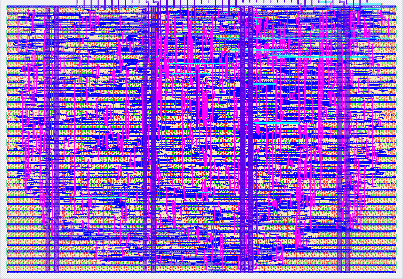
- Author: Fletcher Wilson
- Description: A multiply-accumulate unit that computes the dot product of two signed int8 vectors, time-multiplexing the operands onto a single 8-bit port and reading its 24-bit signed accumulator back over two clock cycles.
- GitHub repository
- Open in 3D viewer
- Open in Tiny Tapeout Explorer
- Clock: 50000000 Hz
How it works
This is a single multiply-accumulate (MAC) unit, which is a fundamental building block of AI accelerators. Although I could only fit one MAC onto a 1x1 tile, modern AI accelerators like Google's TPU construct their matrix multiply units (MXUs) out of grids of up to 256x256 of them, called systolic arrays. These arrays are the engines that make TPUs so good at deep learning computation. Each MAC in the array is a processing element (PE) that initially stores a stationary weight (like a 256x256 snapshot of a neural net layer's weight matrix). Then, activations from the previous layer are fed through the array one column at a time; each PE multiplies its weight by the current activation, adds it to its incoming partial sum, and passes the activation and its new partial sum to its adjacent neighbors. Each MAC column produces one component of the next layer's pre-activation output, which turns out to be a pretty handy way to multiply matrices.
Given the area constraint, however, I had to adapt the role of my MAC so it could still do useful ML math. Instead of receiving an activation from a neighboring PE and multiplying it by a stored weight, my MAC takes two vector components at a time, multiplies them, and adds the product to a running total held in an accumulator register. Basically, one MAC performs the job an entire column of systolic PEs would: computing the dot product of two vectors.
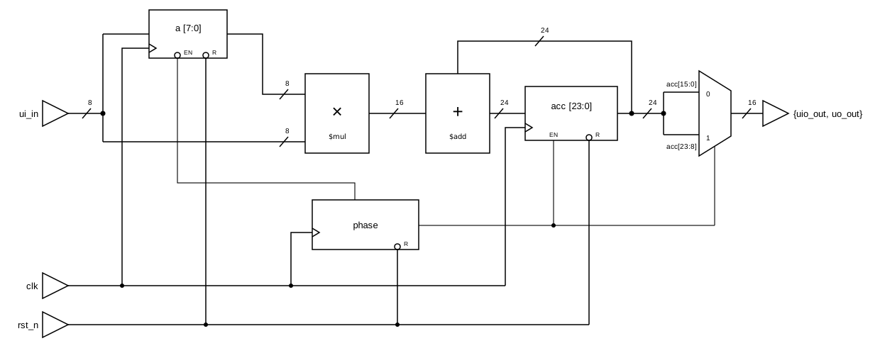
The pin constraints also led to design compromises. Frontier accelerators work mainly with bf16, but at this scale I opted for signed int8 vector components. Multiplying two 8-bit operands needs 16 input bits and only 8 are available, so the operands are time-multiplexed by a two-state FSM: in phase 0 the value on ui_in is captured into an operand register, and in phase 1 the value on ui_in is multiplied by that register and added to the accumulator.
Reading the output presented a similar challenge. A 24-bit accumulator naturally needs more than the 8 dedicated output pins, so all 8 bidirectional pins are configured as output (uio_oe = 8'hFF) and the accumulator is read out over two clock cycles using the same phase bit. In phase 0 the low 16 bits are driven onto {uio_out, uo_out}, and in phase 1 the high 16 bits are driven. Because the accumulator only updates on the phase 1 edge, both halves of a read window come from the same accumulator value. The two windows overlap by one byte, since acc[15:8] leaves on uio_out in phase 0 and on uo_out in phase 1. That falls out of reading three bytes as two 16-bit slices, and it doubles as free error checking: the testbench asserts the two copies agree, so a phase slip surfaces immediately instead of silently corrupting the result.
Note that this means while a component pair is being fed in, the value being driven out is the accumulator as of the previous component pair.
How to test
Interface
| Signal | Dir | Description |
|---|---|---|
ui_in[7:0] |
In | Operand, signed int8 (two's complement) |
uo_out[7:0] |
Out | acc[7:0] in phase 0, acc[15:8] in phase 1 |
uio[7:0] |
Out | acc[15:8] in phase 0, acc[23:16] in phase 1 |
clk |
In | Clock. One component per edge, so one pair every two edges |
rst_n |
In | Active low synchronous reset. Clears accumulator and phase |
All 8 bidirectional pins are held as outputs (uio_oe = 8'hFF), so uio_in is unused.
Reset
To start a new dot product, hold rst_n low for at least one clock edge. This clears the accumulator to zero and forces the FSM to phase 0.
Operation
Interleave the two vectors and present one component per rising edge: x0, y0, x1, y1, ...
| FSM Phase | ui_in |
What Happens | {uio_out, uo_out} |
|---|---|---|---|
| 0 | component of vector 1 (xn) |
captured into the operand register | acc[15:0] |
| 1 | component of vector 2 (yn) |
acc <= acc + xn * yn |
acc[23:8] |
Sample {uio_out, uo_out} in phase 0 for the low half, then in phase 1 for the high half; both refer to the same accumulator value.
Reading the result (see test/helpers.py)
After the final pair, the low half is available immediately, but an additional clock edge is required to return the FSM to phase 1 so the high half can be sampled. That drain edge is a phase 0 edge, so it overwrites the operand register but leaves the accumulator untouched.
Reassemble the two 16-bit windows into the 24-bit accumulator like so:
acc[23:0] = ((hi16 >> 8) << 16) | lo16
Example
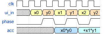
x = [100, -50], y = [-30, 40], so the dot product is 100 * -30 + -50 * 40 = -5000.
Each row is one phase interval: ui_in is the value presented during it, the outputs are what the design drives during it, and the edge that ends it does the capture or the accumulate.
| FSM Phase | ui_in |
Behavior on closing edge | uio_out |
uo_out |
acc value |
|---|---|---|---|---|---|
| 0a | x0 = 0x64 (100) |
a <= 100 |
0x00 |
0x00 |
0x000000 (0) |
| 1a | y0 = 0xE2 (-30) |
acc <= acc + 100 * -30 |
0x00 |
0x00 |
0x000000 (0) |
| 0b | x1 = 0xCE (-50) |
a <= -50 |
0xF4 |
0x48 |
0xFFF448 (-3000) |
| 1b | y1 = 0x28 (40) |
acc <= acc + -50 * 40 |
0xFF |
0xF4 |
0xFFF448 (-3000) |
| 0c | don't care | drain edge, acc untouched |
0xEC |
0x78 |
0xFFEC78 (-5000) |
| 1c | don't care | readout complete | 0xFF |
0xEC |
0xFFEC78 (-5000) |
Reassembling the final phase pair's outputs: hi16 = 0xFFEC, lo16 = 0xEC78, => 0xFFEC78 = -5000.
Range
The accumulator is 24-bit signed, so it holds -8388608 to 8388607. The largest magnitude int8 product is -128 * -128 = 16384, so up to 511 component pairs are guaranteed not to overflow.
IO
| # | Input | Output | Bidirectional |
|---|---|---|---|
| 0 | operand[0] | acc[0] p0 / acc[8] p1 | acc[8] p0 / acc[16] p1 |
| 1 | operand[1] | acc[1] p0 / acc[9] p1 | acc[9] p0 / acc[17] p1 |
| 2 | operand[2] | acc[2] p0 / acc[10] p1 | acc[10] p0 / acc[18] p1 |
| 3 | operand[3] | acc[3] p0 / acc[11] p1 | acc[11] p0 / acc[19] p1 |
| 4 | operand[4] | acc[4] p0 / acc[12] p1 | acc[12] p0 / acc[20] p1 |
| 5 | operand[5] | acc[5] p0 / acc[13] p1 | acc[13] p0 / acc[21] p1 |
| 6 | operand[6] | acc[6] p0 / acc[14] p1 | acc[14] p0 / acc[22] p1 |
| 7 | operand[7] | acc[7] p0 / acc[15] p1 | acc[15] p0 / acc[23] p1 |