288 Two-Channel Reciprocal Counter
288 : Two-Channel Reciprocal Counter
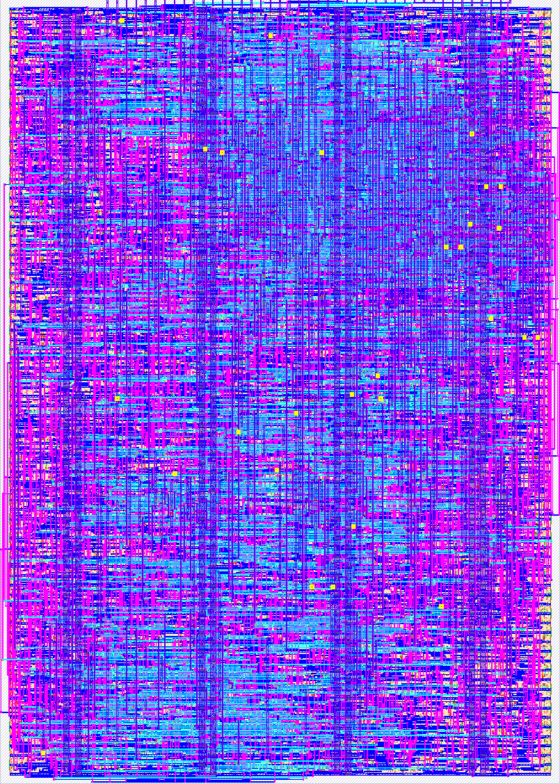
- Author: Brad Pound
- Description: Two-channel reciprocal frequency counter with an SPI register interface
- GitHub repository
- Open in 3D viewer
- Open in Tiny Tapeout Explorer
- Clock: 7200000 Hz
How it works
This project implements a two-channel reciprocal frequency counter for measuring two asynchronous digital oscillator signals.
The Tiny Tapeout system clock is the measurement reference clock. Each external
frequency input passes through a synchronizer before edge detection. The two
channels operate independently and continuously repeat measurements while their
GATE_CYCLES register is non-zero.
For each channel, the design:
- Waits for a synchronized rising edge of the input signal.
- Counts reference-clock cycles while counting the programmed number of input cycles.
- Stores the elapsed reference-clock count in the channel
COUNTregister. - Increments the channel
MEASUREMENT_COUNTregister. - Starts the next measurement on a subsequent input rising edge.
The input frequency can be calculated from:
input_frequency_hz =
    reference_clock_hz * gate_cycles / measured_reference_count
For the Tiny Tapeout design, reference_clock_hz is 7,200,000 Hz.
A channel is disabled when its GATE_CYCLES register is zero. Writing a non-zero
value arms the channel; measurement begins on the next synchronized rising edge.
Configure the timeout register before enabling the channel.
Tiny Tapeout pinout
| Tiny Tapeout pin | Function |
|---|---|
clk |
7.2 MHz reference/system clock |
rst_n |
Active-low reset |
ena |
Design enable; keep high during normal operation |
ui_in[0] |
Channel 0 frequency input |
ui_in[1] |
Channel 1 frequency input |
ui_in[2] |
SPI SCLK |
ui_in[3] |
SPI MOSI |
ui_in[4] |
SPI chip select, active low |
uo_out[0] |
SPI MISO |
Other ui_in, uo_out, and uio pins |
Unused |
The bidirectional Tiny Tapeout pins are not used and their output enables remain disabled.
Register map
All registers are 32 bits wide and use byte addresses.
| Address | Name | Access | Description |
|---|---|---|---|
0x00 |
CH0_GATE_CYCLES |
R/W | Non-zero enables channel 0; zero disables it |
0x04 |
CH1_GATE_CYCLES |
R/W | Non-zero enables channel 1; zero disables it |
0x08 |
CH0_TIMEOUT_REFCOUNT |
R/W | Channel 0 timeout in reference-clock cycles |
0x0C |
CH1_TIMEOUT_REFCOUNT |
R/W | Channel 1 timeout in reference-clock cycles |
0x10 |
CH0_COUNT |
R | Reference-clock count from the latest completed measurement |
0x14 |
CH1_COUNT |
R | Reference-clock count from the latest completed measurement |
0x18 |
CH0_MEASUREMENT_COUNT |
R | Number of completed channel 0 measurements |
0x1C |
CH1_MEASUREMENT_COUNT |
R | Number of completed channel 1 measurements |
0x20 |
CH0_TIMEOUT_COUNT |
R/W1C | Timeout-event counter; write bit 0 as one to clear |
0x24 |
CH1_TIMEOUT_COUNT |
R/W1C | Timeout-event counter; write bit 0 as one to clear |
0x28 |
STATUS |
R/W1C | Live state and sticky diagnostic flags |
STATUS bits:
| Bit | Meaning |
|---|---|
| 0 | Channel 0 active |
| 1 | Channel 1 active |
| 2 | Channel 0 timeout latched |
| 3 | Channel 1 timeout latched |
| 4 | Channel 0 overflow latched |
| 5 | Channel 1 overflow latched |
| 31:6 | Reserved; read as zero |
To clear a sticky timeout or overflow flag, write a one to its corresponding
STATUS bit. Writing zero leaves that flag unchanged.
Startup and counter-initiation sequence
After power-up:
- Hold
rst_nlow for at least ten system-clock cycles. - Set
enahigh. - Release
rst_n. - Keep both
GATE_CYCLESregisters at zero while configuring the design. - Write a suitable timeout value to
CH0_TIMEOUT_REFCOUNTand/orCH1_TIMEOUT_REFCOUNT. - Write the desired non-zero gate-cycle value to each channel that should run.
- Confirm the corresponding
STATUS.ACTIVEbit. - Poll
MEASUREMENT_COUNTuntil it changes, then readCOUNT. - Convert the count to frequency using the equation above.
A useful initial gate-cycle value is:
0x00001000 = 4096 input cycles
The timeout value must be longer than the expected measurement interval. A timeout value of zero should not be used for an enabled channel unless that behavior has been deliberately verified.
To stop a channel, write zero to its GATE_CYCLES register.
SPI interface
The external control interface is an SPI slave connected to the pins listed above. The SPI controller must keep chip select low for the complete command.
Before the final tapeout submission is tagged, record the verified SPI mode,
bit order, byte framing, read-command value, write-command value, and chip-select
timing here. These details must match both spi_register_interface.v and the
hardware-validation procedure. Do not rely only on memory when the boards arrive.
The executable SPI transaction reference is the cocotb test in test/test.py.
Preserve that test with the tagged tapeout revision.
How to test
The functional cocotb tests are located in test/test.py.
From the test directory:
make clean
make
Before submitting or revising the Tiny Tapeout project, verify:
- Reset behavior
- SPI write and readback of all four configuration registers
- Channel 0 measurement
- Channel 1 measurement
- Simultaneous two-channel operation
- Disabling one channel without disturbing the other
- Measurement counters incrementing
- Timeout detection and recovery
- Timeout-counter clearing
- Sticky timeout clearing
- Overflow behavior and sticky-overflow clearing
- Unused outputs are driven to known values
uio_oeremains zero
External hardware validation
The production SPI path should be exercised on the FPGA before the final submission revision is frozen.
The FPGA test should use an SPI master to drive physical jumper wires connected
to the FPGA pins running the same spi_register_interface slave RTL used in the
ASIC design:
PC / UART command console
    -> FPGA SPI master
    -> physical jumper wires
    -> FPGA SPI slave
    -> register file
    -> reciprocal counter channels
The existing UART debug-register path bypasses the SPI slave and therefore does not, by itself, verify SPI clocking, chip-select timing, MOSI sampling, MISO shifting, transaction framing, or bit alignment.
Files to preserve with the submitted revision
Keep the following together under a release tag or submission commit:
- RTL source files listed by
info.yaml - Tiny Tapeout top-level wrapper
info.yamlsrc/config.json- This
info.md - Cocotb source tests
- Gate-level test results
- Successful precheck report
- Successful hardening logs
- Final GDS submission artifact
- Gate-level netlist
- SDF timing file
- A note identifying the exact Git commit submitted through the Tiny Tapeout portal
When the manufactured test boards arrive, begin from the tagged commit rather than the development branch.
IO
| # | Input | Output | Bidirectional |
|---|---|---|---|
| 0 | CH0_SIGNAL | SPI_MISO | |
| 1 | CH1_SIGNAL | ||
| 2 | SPI_SCLK | ||
| 3 | SPI_MOSI | ||
| 4 | SPI_CS_N | ||
| 5 | |||
| 6 | |||
| 7 |