873 Dot product engine
873 : Dot product engine
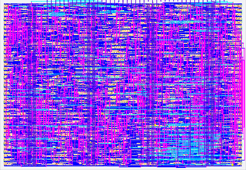
- Author: Andre Machoski
- Description: FSM-driven dot product engine
- GitHub repository
- Open in 3D viewer
- Open in Tiny Tapeout Explorer
- Clock: 10000000 Hz
How it works
This design is a small digital datapath controller built around a finite-state machine (FSM). It receives input data on ui_in, controls a memory bank, performs arithmetic through a multiply-accumulate block, and exposes the current status and result through the Tiny Tapeout IO ports.
The top-level module tt_um_andre_dpe connects:
ui_in[7:0]: input data busuo_out[7:0]: output data busuio_in[7:0]: control and debug inputsuio_out[7:0]: status output bitsuio_oe[7:0]: IO enable configuration
The FSM supports several modes through the control bits ctl[1:0]:
- Idle: waits for new operations
- Work: processes the selected datapath operation
- Debug: exposes internal values or memory bank state through
data_out
The design includes:
- a register/memory bank for storage
- a MAC unit for multiply-accumulate operations
- debug selection logic to read specific memory or intermediate values
- status flags indicating whether the FSM is idle, busy, has data ready, or hit an internal error
In practice, the chip acts as a compact programmable control block for arithmetic and memory access, intended as a learning-oriented Tiny Tapeout implementation.
How to test
The project is tested with a cocotb-based Verilog simulation.
From the test directory, run:
make
This will compile the RTL, run the testbench, and produce a waveform such as tb.vcd or tb.fst depending on the current dump format settings.
The testbench drives the clock, reset, control bits, debug selector, and input data, then checks:
- reset behavior
- FSM state transitions
- status changes
- output result values
- debug readback from the memory or datapath
To inspect the waveform, open the generated file with GTKWave:
gtkwave tb.vcd
or
gtkwave tb.fst
External hardware
No external hardware is required for simulation.
This project is intended to run in the Tiny Tapeout environment and can be tested entirely through the supplied Verilog simulation setup.
IO
| # | Input | Output | Bidirectional |
|---|---|---|---|
| 0 | DATA_IN[0] | DATA_OUT[0] | STATUS[0] |
| 1 | DATA_IN[1] | DATA_OUT[1] | STATUS[1] |
| 2 | DATA_IN[2] | DATA_OUT[2] | DEBUG_SEL[0] |
| 3 | DATA_IN[3] | DATA_OUT[3] | DEBUG_SEL[1] |
| 4 | DATA_IN[4] | DATA_OUT[4] | DEBUG_SEL[2] |
| 5 | DATA_IN[5] | DATA_OUT[5] | DEBUG_SEL[3] |
| 6 | DATA_IN[6] | DATA_OUT[6] | CTL[0] |
| 7 | DATA_IN[7] | DATA_OUT[7] | CTL[1] |