941 TTSKY-SPSRAM-direct
941 : TTSKY-SPSRAM-direct
- Author: Staf Verhaegen
- Description: Sky130 single port SRAM with pins connected directly to TT tile pins.
- GitHub repository
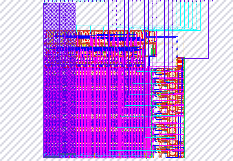
- Open in 3D viewer
- Clock: 66000000 Hz
How it works
This design contains a single port SRAM block with pins connected directly to TT tile pins. This allows to use this design directly as a SRAM block.
The included block has 128 words of 8 bits. These are the pins for the block:
- a (7 bit): address
- we (1 bit): write enable signal indicating a read or write operation
- d (8 bit): input data
- q (8 bit): output data
- clk: clock for performing an operation
On each rising edge of the clock an operation is performed on the memory. A read is done when we is 0, while a write operation is done when it is 1. On the rising edge of the clock the a and d signals are latched into an internal buffer. For a read operation the data for the provided address is put into the q signal, the d signal is ignored. For a write operation the value of the d signal is put in the given address. The write operation is write-through meaning that also q will get the value of d during the operation.
How to test
You can test the block yourself by providing the right inputs for a read or write operation. One can check if data written to a certain location is later on read back with a read operation on the same address.
IO
| # | Input | Output | Bidirectional |
|---|---|---|---|
| 0 | a[0] | q[0] | d[0] |
| 1 | a[1] | q[1] | d[1] |
| 2 | a[2] | q[2] | d[2] |
| 3 | a[3] | q[3] | d[3] |
| 4 | a[4] | q[4] | d[4] |
| 5 | a[5] | q[5] | d[5] |
| 6 | a[6] | q[6] | d[6] |
| 7 | we | q[7] | d[7] |