520 Configurable Self-biasing Miller-compensated OTA
520 : Configurable Self-biasing Miller-compensated OTA
- Author: atenfyr
- Description: A single-ended two-stage Miller-compensated OTA with a self-biasing beta multiplier current reference circuit and configurable compensation on SKY 130nm
- GitHub repository
- Open in 3D viewer
- Clock: 1000 Hz
How it works
This project is a single-ended two-stage Miller-compensated OTA with a self-biasing beta multiplier current reference circuit and configurable compensation on SKY 130nm.
Pins
| Name | No. | Description |
|---|---|---|
| OUT | ua[0] | OTA output |
| IN+ | ua[1] | OTA non-inverting input |
| IN- | ua[2] | OTA inverting input |
| COMP_S0 | ui[0] | Miller compensation mode select 0 (MSB) |
| COMP_S1 | ui[1] | Miller compensation mode select 1 (LSB) |
| BEAT | uo[0] | Heartbeat status signal; tied to CLK |
| COMP_S1 | COMP_S0 | Behavior |
|---|---|---|
| 0 | 0 | Compensation capacitance of 1.5 pF (default) |
| 0 | 1 | Compensation capacitance of 3.5 pF |
| 1 | 0 | Compensation capacitance of 5.5 pF |
| 1 | 1 | DNU |
Specifications
Absolute Maximum Ratings
| Name | Min | Max | Unit |
|---|---|---|---|
| Supply voltage, VDD | 0 | 1.95 | V |
| Supply voltage, VSS | 0 | 1.95 | V |
| Input voltage, any input | 0 | 1.95 | V |
| Operating temperature | -40 | 100 | °C |
Recommended Operating Conditions
| Name | Min | Max | Unit |
|---|---|---|---|
| Supply voltage, VDD | 1.7 | 1.9 | V |
| Supply voltage, VSS | 0 | 0 | V |
| Operating temperature | -40 | 85 | °C |
Electrical Characteristics
All reported characteristics are based on pre-layout simulations across PVT corners with COMP_S1 = COMP_S0 = 0, 1.7 < VDD < 1.9, and -40 °C < T < 85 °C. Input values and temperatures outside of this range may cause values beyond the minimum or maximum values provided below.
| Name | Test Condition | Min | Typ. | Max | Unit |
|---|---|---|---|---|---|
| Vio, input offset voltage | Vo = 900 mV, full temp. range | 0.1 | 3 | mV | |
| Vos, maximum peak-to-peak output voltage swing | Vo,DC = 900 mV, THD < 5%, full supply voltage range, full temp. range | 0.7 | 1.3 | V | |
| Avo, small-signal differential voltage amplification | Vin,cm = 900 mV, full temp. range | 1 | 4.5 | V/mV | |
| gm, small-signal differential transconductance | Vin,cm = 900 mV, RL = 10 kΩ, full temp. range | 50 | 200 | mS | |
| GBW, gain-bandwidth product | measured at corner frequency, full temp. range | 5 | 20 | 30 | MHz |
| PM, phase margin | measured at unity-gain bandwidth, full temp. range, C_L = 10 pF | 35 | 50 | ° | |
| ro, small-signal output resistance | full temp. range | 1 | 6 | 12 | kΩ |
| CMRR, common-mode rejection ratio | full temp. range | 50 | 70 | dB | |
| PSRR+, power supply rejection ratio (VDD) | VDD = 1.8 V, full temp. range | 45 | 80 | dB | |
| PSRR-, power supply rejection ratio (VSS) | VSS = 0 V, full temp. range | 45 | 80 | dB | |
| Isc, short-circuit output current | full temp. range | 5 | 15 | mA | |
| P, passive power consumption | full temp. range, Vo = 0 V, no load | 0.6 | 2 | mA |
Schematics
OTA
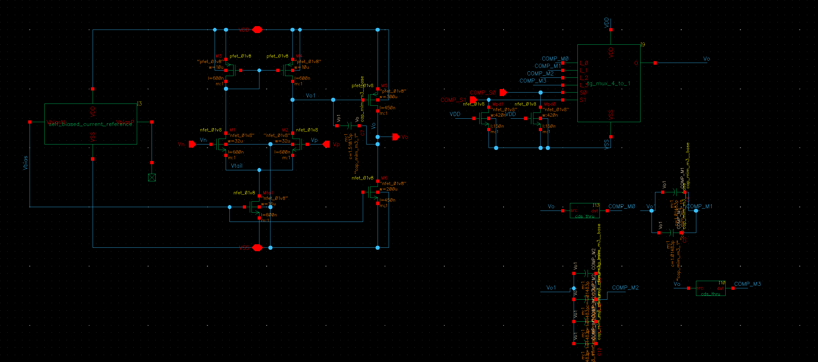
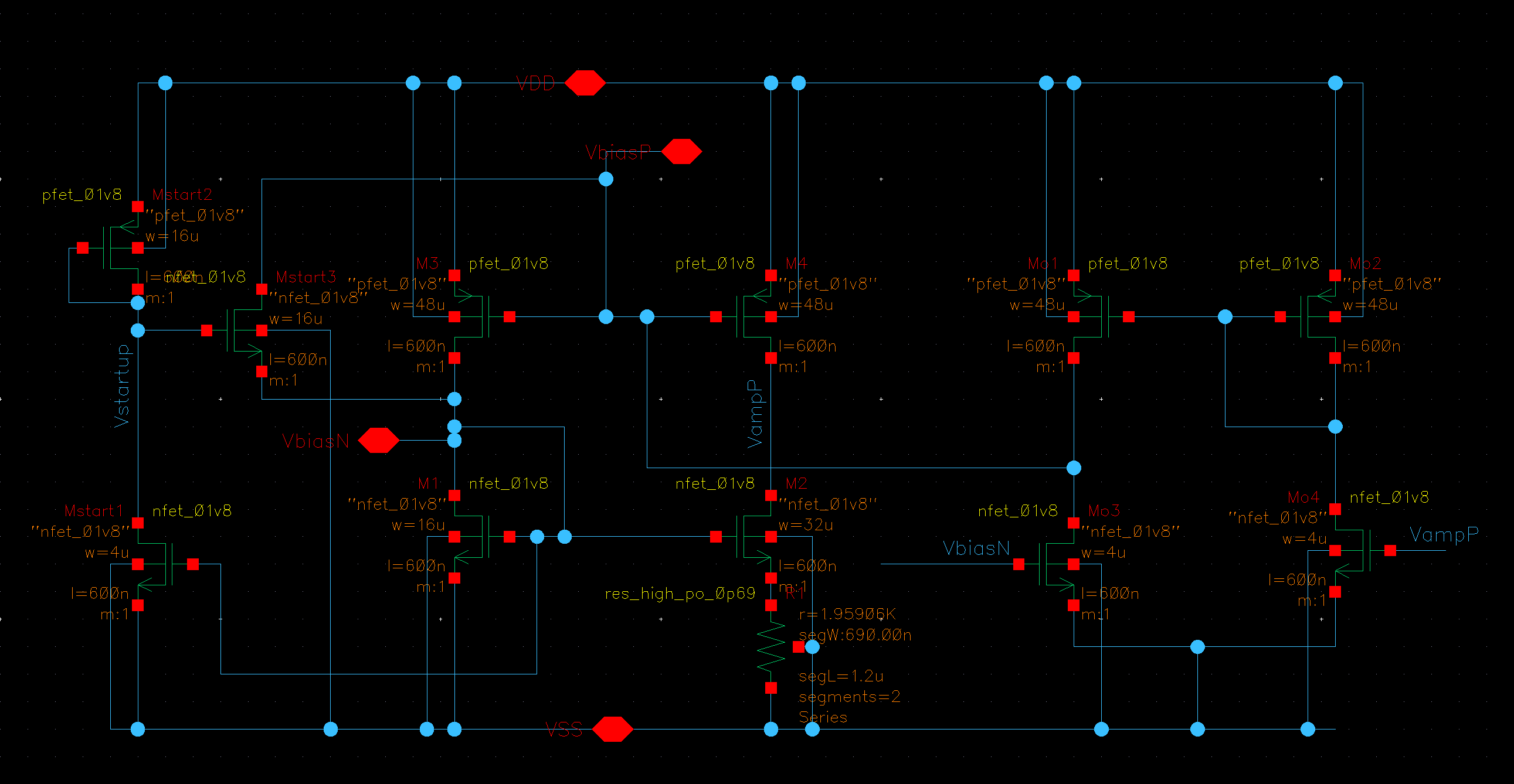
self_biased_current_reference
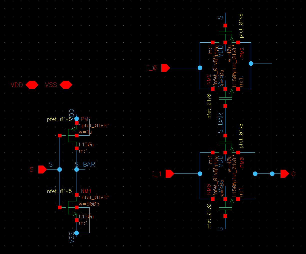
tg_mux_4_to_1
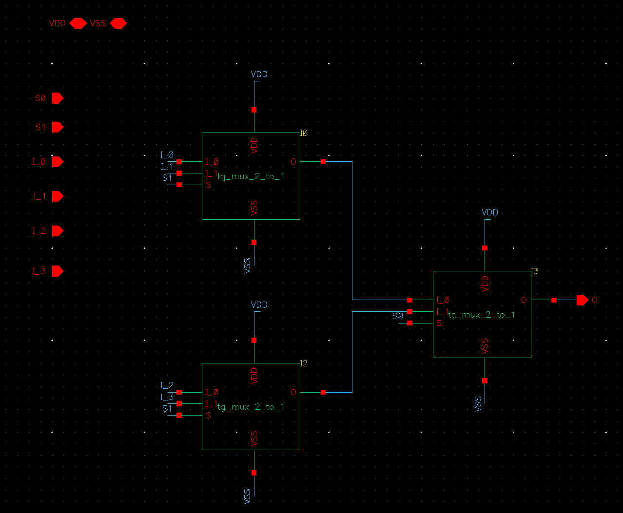
tg_mux_2_to_1
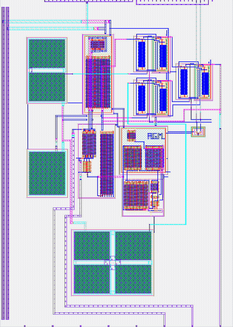
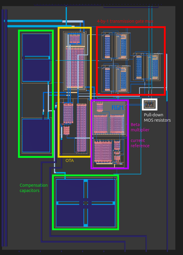
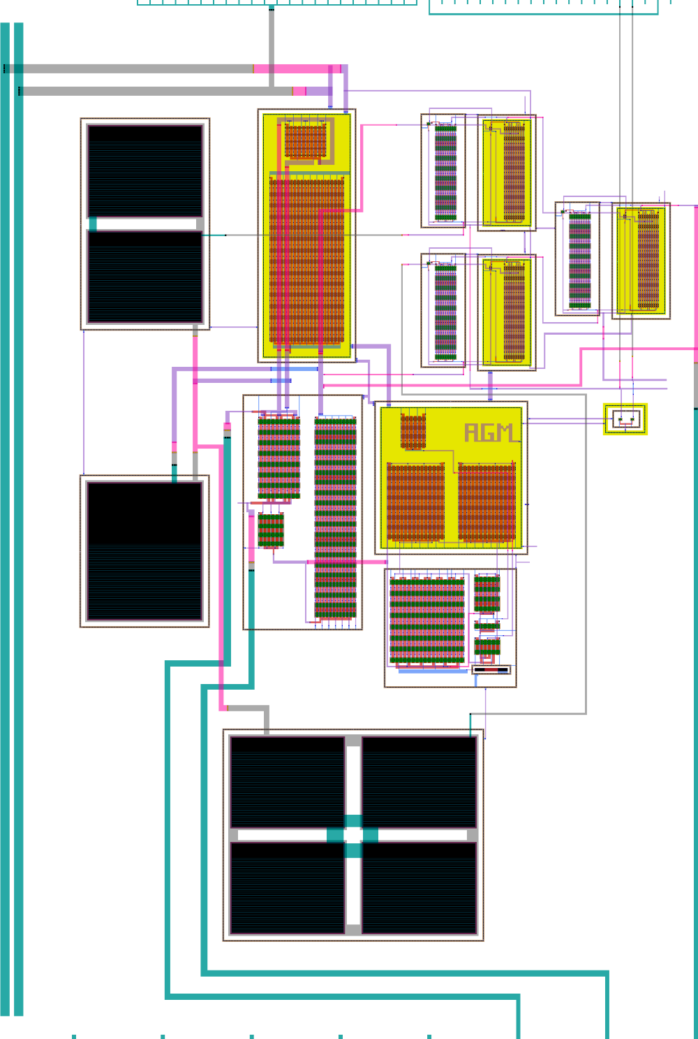
Layout
How to test
This OTA should be operated in a feedback configuration. One common configuration to verify basic operation could be to tie the inverting input (ua[2]) to the output (ua[0]) to create a unity-gain buffer, where any input signal fed into the non-inverting input (ua[1]) should be matched at the output. Gain-bandwidth product (GBW) can be estimated by finding the frequency at which the voltage gain begins to drop below 1 V/V in this configuraton.
License
Copyright (c) atenfyr, 2026, under the Apache License 2.0.
IO
| # | Input | Output | Bidirectional |
|---|---|---|---|
| 0 | COMP_S0 | BEAT | |
| 1 | COMP_S1 | ||
| 2 | |||
| 3 | |||
| 4 | |||
| 5 | |||
| 6 | |||
| 7 |
Analog pins
ua | PCB Pin | Internal index | Description |
|---|---|---|---|
| 0 | B1 | 7 | OUT |
| 1 | B3 | 9 | IN+ |
| 2 | B2 | 8 | IN- |