517 uart
517 : uart
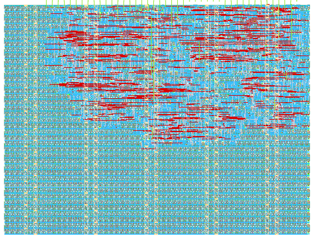
- Author: bella
- Description: basic uart w rx and tx
- GitHub repository
- Open in 3D viewer
- Open in Tiny Tapeout Explorer
- Clock: 49152000 Hz
UART (Universal Asynchronous Receiver + Transmitter) : A Tiny Tapeout Project
How it works
This project implements a simple UART (Universal Asynchronous Receiver + Transmitter). It's capable of independently transmitting and receiving 8-bit serial data (8-N-1).
| Field | Value |
|---|---|
| Data bits | 8 |
| Parity | None |
| Stop bits | 1 |
The design is split into four modules:
-
tt_um_blonghi_uart- the top-level wrapepr that maps pins to signals and instantiates the 3 following modules. -
baud_rate_gen- generates two enable ticks from the system clock. 'tx_counter' wraps around at 5119, producing 'tx_enb' (one pulse per baud period). 'tx_counter' resets every 'tx_sync' pulse (the start of a new frame), keeping TX bit timing aligned. 'rx_counter' wraps around at 319 (1/16th of 'tx_counter's range) This produces 'rx_enb' at 16x the rate to allow the receiver to oversample and locate the center of each incoming bit. 'rx_counter' resets every 'rx_sync' pulse (start-bit detection), keeping RX sampling aligned. -
transmitter- FSM that on write request serializes an 8-bit byte onto the tx line as: start bit, 8 data bits (LSB first), then a stop bit.
stateDiagram-v2
direction LR
    [*] --> IDLE
    IDLE --> START: wr_enb
    START --> DATA: tx_enb
    DATA --> STOP: 8 bits transmitted
    STOP --> IDLE: tx_enb
receiver- FSM that watches the rx line for a falling edge (start bit) then samples 8 data bits at the center od each bit period (16x oversampling to find bit-center), then checks for the stop bit and pulses rx_valid for one cycle with the received byte on rx_data.
stateDiagram-v2
direction LR
    [*] --> IDLE
    IDLE --> START: falling edge
    START --> DATA: rx_enb
    DATA --> STOP: 8 bits received
    STOP --> IDLE: valid stop bit
Limitations
- No parity bit.
- If there is a bad frame, it is simply never latched with no downstream indication the error occurred.
rx_datais split between two buses:uio_outanduo_out
Pin mappings
TX (transmit)
| Signal | Pin | Direction |
|---|---|---|
tx_data |
ui_in[7:0] |
input |
wr_enb |
uio_in[0] |
input |
tx |
uo_out[0] |
output |
RX (receive)
| Signal | Pin | Direction |
|---|---|---|
rx |
uio_in[1] |
input |
rx_valid |
uo_out[1] |
output |
rx_data[1:0] |
uo_out[3:2] |
output |
rx_data[7:2] |
uio_out[7:2] |
output |
Note: keep in mind that rx_data is split across two separate output buses
Unused / fixed
| Signal | Pin | Value |
|---|---|---|
| — | uio_in[7:2] |
unused |
| — | uo_out[7:4] |
tied to 0 |
| — | uio_out[1:0] |
tied to 0 |
uio_oe |
— | fixed 8'b1111_1100 |
Note: uio_oe is fixed since I needed to accommodate 6 continuous
output pins for the upper bits of rx_data and 2 input pins for wr_enb
and rx.
Baud rate assumptions
My Main Assumptions
- System clock: 49.152 MHz
- Target baud rate: 9600
- TX: exactly 5120 clock cycles per bit
- RX: 16x oversampling
- RX: exactly 320 clock cycles per tick
- RX samples near tick 8
The Math:
The clock runs at $49,152,000$ Hz (not a round 50 MHz, see note below), which means $49,152,000$ clock cycles per second.
9600 baud means $9600$ bits per second.
So the number of clock cycles in one bit is $\frac{49,152,000}{9600} = 5120$.
For RX, I use 16x oversampling, meaning there are 16 RX ticks for every bit: $\frac{5120}{16} = 320$.
So the RX counter uses exactly 320 clock cycles per RX tick.
The receiver then counts these 16 RX ticks and samples the actual RX signal around tick 8.
Note: 50,000,000 / 9600 isn't a whole number (5208.33), which causes a small timing error. 49,152,000 was chosen specifically because it divides evenly at both levels: once by 9600 for the bit period, and again by 16 for the RX tick.
This all came out of FPGA testing, where a rounding mismatch (27MHz clock, 9600 baud) caused decode errors until a cleanly dividing rate was used instead.
How to test
RTL simulation
cd test
pip install -r requirements.txt
make -B
GLS
Requires one-time PDK setup which can be a headache ;-;.
Once the PDK is set up, this is the whole sequence. Run it again every time you change a .v file, since hardening makes a new netlist and the copy sitting in test/ goes stale.
export PDK_ROOT=/path/to/IHP-Open-PDK
export PDK=ihp-sg13cmos5l
export LIBRELANE_TAG=3.0.0rc1

# from the repo root
./tt/tt_tool.py --harden --ihp

cd test
make -B                  # RTL simulation

TOP_MODULE=$(cd .. && ./tt/tt_tool.py --print-top-module --ihp)
cp ../runs/wokwi/final/nl/$TOP_MODULE.nl.v gate_level_netlist.v

make -B GATES=yes        # gate-level simulation
IO
| # | Input | Output | Bidirectional |
|---|---|---|---|
| 0 | tx_data[0] | tx | wr_enb |
| 1 | tx_data[1] | rx_valid | rx |
| 2 | tx_data[2] | rx_data[0] | rx_data[2] |
| 3 | tx_data[3] | rx_data[1] | rx_data[3] |
| 4 | tx_data[4] | rx_data[4] | |
| 5 | tx_data[5] | rx_data[5] | |
| 6 | tx_data[6] | rx_data[6] | |
| 7 | tx_data[7] | rx_data[7] |