161 FPU-130
161 : FPU-130
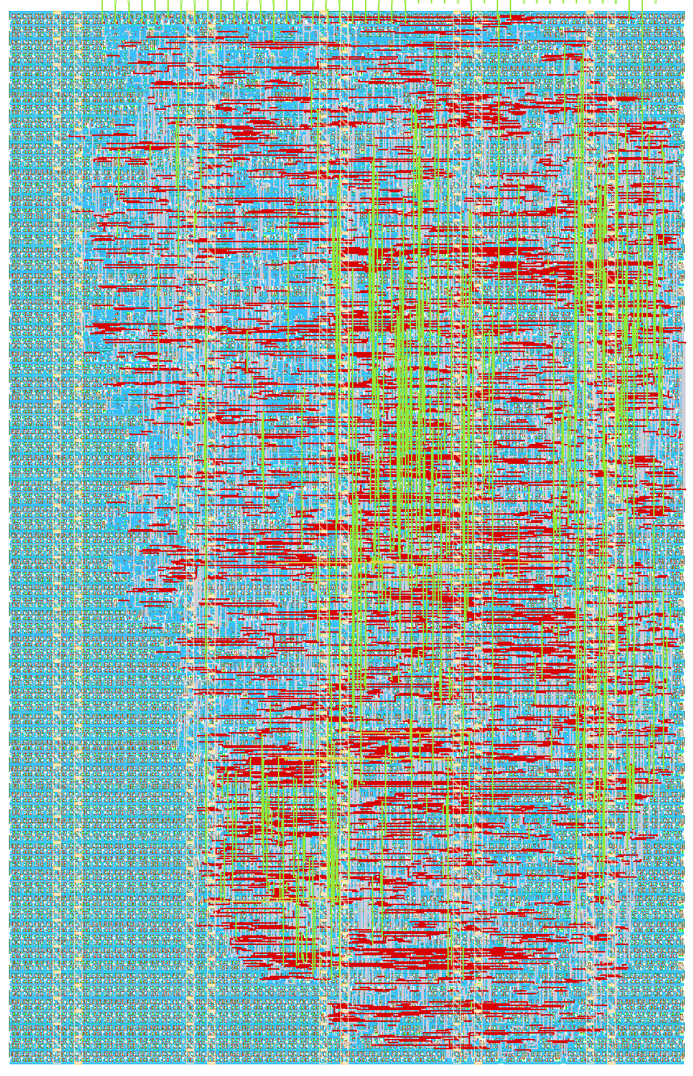
- Author: Aarush & Yogith
- Description: a FPU for the 16bfloat format that takes commands over SPI
- GitHub repository
- Open in 3D viewer
- Open in Tiny Tapeout Explorer
- Clock: 50000000 Hz
How it works
FPU-130 is an SPI-controlled arithmetic coprocessor for the 16-bit
bfloat16 format. A bfloat16 value contains one sign bit, eight exponent
bits, and seven fraction bits. It is also the upper 16 bits of an IEEE-754
single-precision value; for example, 1.0, 2.0, and 3.0 are encoded as
0x3f80, 0x4000, and 0x4040 respectively.
The supported operations are:
| Opcode | Operation | Description |
|---|---|---|
000 |
ADD | A + B |
001 |
SUB | A - B |
010 |
MUL | A * B |
011 |
DIV | A / B |
100 |
NEG | -A |
101 |
ABS | abs(A) |
110 |
SLT | 1.0 when A < B, otherwise 0.0 |
111 |
NOP | No arithmetic writeback |
The SPI interface uses mode 0, active-low chip select, and MSB-first byte ordering. The command byte is arranged as follows:
| Bits | Field |
|---|---|
[7:5] |
Opcode |
[4] |
Accumulator enable |
[3] |
Arity: 0 for unary, 1 for binary |
[2:0] |
Three-bit request tag |
A binary frame contains six bytes:
[command] [A high] [A low] [B high] [B low] [CRC-8]
A unary frame contains four bytes:
[command] [A high] [A low] [CRC-8]
The final byte is CRC-8/AUTOSAR, calculated over every preceding byte in the
frame with polynomial 0x2f, initial value 0xff, and final XOR value
0xff.
The FPU response is 24 bits, MSB first:
[status] [result high] [result low]
The status byte contains the echoed tag in bits [7:5], CRC/SPI error in bit
4, a valid marker in bit 3, underflow in bit 2, overflow in bit 1, and NaN in
bit 0. SPI is full duplex, but an operation cannot be computed until its full
request has arrived. Consequently, the bytes received while sending a request
belong to the previous result. Clock the completed result out in a following
transaction, or pipeline it with the next command.
How to test
Select the design, provide its system clock, pulse rst_n low, and then leave
rst_n high. Connect an SPI controller as follows:
| Signal | Tiny Tapeout pin | Direction relative to FPU-130 |
|---|---|---|
| CS (active low) | uio[0] |
Input |
| MOSI | uio[1] |
Input |
| MISO | uio[2] |
Output |
| SCLK | uio[3] |
Input |
Use SPI mode 0 and start with a low SPI clock frequency for bring-up. The SPI signals pass through synchronizers clocked by the project clock, so the project clock must remain active and substantially faster than SCLK.
As a known-good test, add 1.0 to 2.0 with tag zero:
Request: 08 3f 80 40 00 34
Here 0x08 selects binary ADD, 0x3f80 is 1.0, 0x4000 is 2.0, and
0x34 is the frame CRC. After sending the request, deassert CS and allow the
FPU time to finish. For initial testing, waiting at least 100 project-clock
cycles is conservative. Assert CS again and provide 24 SCLK cycles. The
expected response is:
Response: 08 40 40
0x08 is a clean status byte with its valid marker set, and 0x4040 is the
bfloat16 representation of 3.0. The first transaction after reset does
not return the result being submitted; it is produced only after that request
has been received and processed.
External hardware
Testing requires a Tiny Tapeout carrier or compatible FPGA setup, an SPI controller like ESP32. Find the code for ESP32 on https://github.com/140oo041/FPU-micro-processor
Known Defects
Sometimes there may be a 2 bit offset using this interface. The best way to interface is to schedule operations together, and then send one big SPI transfer. After receveing the data, and CS goes down, reset the board.
IO
| # | Input | Output | Bidirectional |
|---|---|---|---|
| 0 | CS SPI | ||
| 1 | MOSI SPI | ||
| 2 | MISO SPI | ||
| 3 | SCK SPI | ||
| 4 | |||
| 5 | |||
| 6 | |||
| 7 |