426 PRISM with Risc-V (TinyQV) SoC
426 : PRISM with Risc-V (TinyQV) SoC
- Author: Ken Pettit with Michael Bell's TinyQV
- Description: A PRISM controller suported by a TinyQV Risc-V SoC
- GitHub repository
- Open in 3D viewer
- Open in Tiny Tapeout Explorer
- Clock: 64000000 Hz
How it works
This tile is PRISM, a Programmable Reconfigurable Indexed State Machine: a protocol engine whose states, transitions, inputs and outputs are loaded at run time as a bitstream compiled from an ordinary Verilog state machine. A small RISC-V core, TinyQV, sits beside it as the host processor. PRISM does the bit- and byte-level timing of a protocol in hardware, one state transition per clock; the CPU loads the state machine, configures the datapath, moves data through the FIFOs and runs the protocol's upper layers. Protocols that have run on it in simulation include UART, SPI (slave, and single- or quad-lane master), I2C (master and slave), 1-Wire, WS2812, a quadrature encoder, a 24-bit GPIO expander and a USB low-speed device; the 8x4 build with SRAM FIFOs adds 10BASE-T Ethernet transmit and receive.
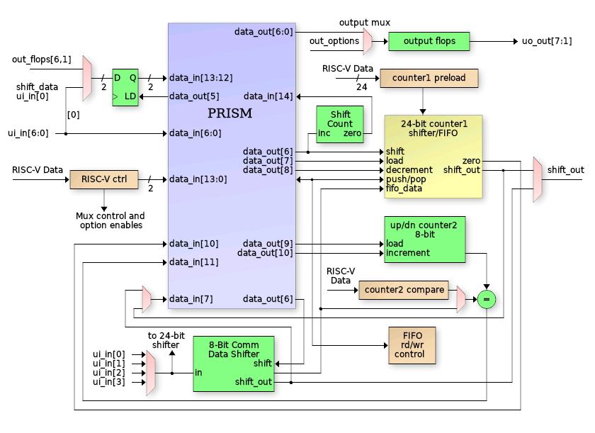
What is on the tile
- The PRISM core: 32 states, each described by a 128-bit State Execution
Word (STEW). Six input muxes pick from 32 inputs; two 3-input LUTs form an
if / else if / elsedecision per state; each branch drives its own set of 21 outputs; two more 2-input LUTs drive conditional outputs that follow the inputs within a state. - Two shards: the machine can be fractured into two independent 16-state state machines, each with its own state index, inputs, outputs, datapath, FIFOs and host interrupt, talking to each other through semaphores. Unfractured, one 32-state machine owns everything.
- A datapath per shard: a 24/32-bit counter that doubles as a wide shift register, an 8-bit counter with compare, an 8-bit communication shifter (1 to 4 bits per shift), four constants, a 64-byte FIFO (32 in the smaller build), a CRC unit (8/16/32) that doubles as a 32-bit up/down counter with compare, a Manchester bit recoverer, an edge-clocked sampler, edge-capture flops and a second timer.
- CFGMEM: eight latch-array macros (16 rows x 32 bits each) built with a DFFRAM-style flow hold the state table; the CPU loads them through a shift chain per bank.
- A debugger with halt, single step and condition-qualified breakpoints per shard. This 5x4 tile is the SRAM-less build of the design: the 8x4 tile adds a 2 KB SRAM FIFO per shard and an execution tracer into them.
- TinyQV: RV32EC + Zcb + Zicond, code from a QSPI flash and data in QSPI PSRAM, with a UART, a debug UART and GPIO.
PRISM: the Programmable Reconfigurable Indexed State Machine
PRISM executes a state machine that is loaded at run time. The state
machine is written as an ordinary Verilog Mealy FSM, a chroma, and
compiled by a Yosys backend into a table of 32 State Execution Words
(STEWs) of 128 bits plus the configuration words for the datapath. The
host CPU loads the table, configures the datapath, enables the machine, and
from then on PRISM makes one decision per clock from its 32 inputs and
drives 21 outputs, with no software in the loop. This document describes
the machine on the IHP sg13g2 8x4 tile. The design record with the
reasoning behind each feature is prism_interface.md;
the register constants used by the tests are in
test/user_peripherals/prism/regs.py.
1. At a glance
| States | 32, in two banks of 16 |
| State word | 128 bits (STEW), from the CFGMEM latch macros |
| Inputs | 32 per shard, 6 input muxes per state |
| Decision | two 3-input LUTs per state: if (tree 0), else if / else (tree 1) |
| Outputs | 21 per shard, a separate set for the resting state and for each of the two branches |
| Conditional outputs | two per shard, each a 2-input LUT of the current inputs |
| Fracture | one 32-state machine, or two independent 16-state shards |
| Per shard | 24/32-bit count1 (counter or wide shifter), 8-bit count2 with compare, 8-bit comm shifter, 4 constants, constant table, 64-byte FIFO, 2 KB SRAM FIFO, CRC / counter unit, Manchester recoverer, edge sampler, 4 edge-capture flops, timer 2, interrupt |
| Debug | halt, single step, two breakpoints per shard with entry / if / else-if / exit conditions, live and registered readback |
| Trace | 1024 entries per SRAM (2048 with both), entry = state, decision inputs, outcome |
| Host | TinyQV, 512-byte register region at 0x8000200; CFGMEM loader at 0x8000100 |
Variants of the same RTL: the CMOS5L tile has 16-byte flop FIFOs and neither the counter mode nor the 32-bit FIFO access; the sg13g2 5x4 tile has no SRAMs, so no SRAM FIFOs and no tracer.
2. The core
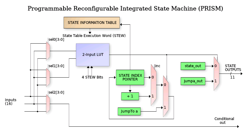
The current state index (SI, 5 bits) addresses the State Information
Table; the word that comes back is the STEW for that state. While the
machine sits in a state the STEW's default outputs drive the 21 outputs.
Six 5-bit fields of the STEW select six of the 32 inputs. Muxes 0-2 feed
tree 0, a 3-input LUT programmed by 8 STEW bits; muxes 3-5 feed tree 1.
Tree 0 is the chroma's if: when its LUT is true the machine jumps to the
tree 0 target state and drives the tree 0 outputs for that one clock.
Tree 1 is the else if (or a plain else, compiled as an always-true
LUT): it is taken when it matches and tree 0 does not, with its own target
and its own outputs. When neither fires the machine stays. Two more LUTs,
2 inputs each (cond 0 from muxes 1 and 4, cond 1 from muxes 3 and 5), drive
the conditional outputs, whose value follows the inputs within the
state; a chroma writes them as cond_out[0] = 1'b0; if (x) cond_out[0] = 1'b1;.
The inc bit starts or continues the auto-loop: in a state with inc
set, "no match" moves to the next state instead of staying, and the first
such state is remembered; a later state without inc and no match returns
there. The compiler emits it for the idiom "a chain of tests with a
trailing else -> next state", so a scan over several states costs no
decision tree.
STEW layout (chromas/tinyqv32.cfg):
| bits | field |
|---|---|
| 0 | inc |
| 30:1 | mux 0 .. mux 5 input selects, 5 bits each |
| 35:31 | tree 1 jump target |
| 40:36 | tree 0 jump target |
| 61:41 | default outputs |
| 82:62 | tree 1 outputs |
| 103:83 | tree 0 outputs |
| 111:104 | tree 0 LUT3 |
| 119:112 | tree 1 LUT3 |
| 123:120 | cond 0 LUT2 |
| 127:124 | cond 1 LUT2 |
3. Shards and fracturing
The 32 states live in two banks of 16: bank A (CFGMEM "lo" macros, states
0-15) and bank B ("hi", states 16-31). Unfractured (FRAC_CFG = 0)
shard 0 is the whole machine: its SI selects the bank with its top bit,
shard 1's index register silently tracks shard 0's low bits so both banks
are always addressed without a mux, and shard 1's datapath idles (its
registers stay accessible, and shard 0 can use shard 1's FIFO as a second
FIFO, section 8). Fractured (FRAC_CFG = 1) each bank is an independent
16-state machine with its own SI, its own 32 inputs, its own 21 outputs, its
own datapath, its own interrupt and its own debugger. A chroma compiled
with tinyqv32_shard.cfg (16 states) loads into either bank.
The two shards see each other in three ways:
- Semaphores: OUT_SEMA_SET (output 19) in one shard sets a sticky flag the other shard reads as input 24 and clears with its OUT_SEMA_CLEAR (output 15). If set and clear meet in the same cycle the receiving shard's CFG0[24] decides who wins. The host reads both flags in INT_STATUS[3:2].
- Input 25: the other shard is halted (registered).
- Pins: each shard's PINMUX names a source for every uo_out[7:1] pin, or code 7 for "not mine". A pin claimed by shard 0 goes to shard 0, otherwise to shard 1, otherwise to GPIO; a pin freezes while its owning shard is halted.
The output and conditional-output masks at 0x44-0x50 gate which of a shard's outputs reach its datapath while fractured; they reset to zero, so a fractured configuration must set them.
4. Inputs
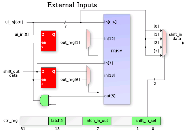
Every shard has the same 32 inputs. Bits 0-15 keep the meaning of the original two-tile PRISM so old chromas read the same; 16 and up carry the newer features.
| input | meaning |
|---|---|
| 0-6 | ui_in[6:0], after the shard's synchroniser select: CFG0[19:18] = 0 two flops, 1 one flop, 2 raw |
| 7 | shift_data: the serial-out bit of the selected shifter |
| 8, 9 | host_in[1:0], written by the host (a byte write to +0x15 toggles bit 0 and clears the interrupt) |
| 10 | count1_term: count1 reached 0 counting down, or the preload / roll-over counting up |
| 11 | count2_cmp: count2 >= COMPARE |
| 12, 13 | latched_in: {shift_data, cond_out[0]} captured by OUT_LATCH, or the latched outputs with CFG0[7], or two FSM flags with CFG0[29] |
| 14 | shift_term: the shift count reached the configured length |
| 15 | count2 == comm |
| 16-19 | input slots, default the four edge-capture flops in_prev[3:0] (section 4.1) |
| 20, 21 | own FIFO flags: empty and full by default, CFG1[25:24] / [27:26] pick almost-empty / almost-full / the other side |
| 22 | crc_ok: the CRC equals CRC_EXPECTED; in counter mode, count >= CRC_EXPECTED |
| 23 | count1_wrap: count1 rolled over counting up |
| 24 | semaphore set by the other shard |
| 25 | the other shard is halted |
| 26, 27 | FIFO B's flags for shard 0 unfractured (CFG1[29:28] / [31:30]); 0 otherwise |
| 28-31 | input slots, default 0; input 28's default is the timer 2 tick (section 11) |
Input slots (CFG2, four bits per slot for inputs 16-19 and 28-31) let a chroma bring other signals into a state's decision: code 0 the slot's default, 1-4 in_prev[0..3], 5-12 comm[0..7] (so the decision trees decode a received byte, a USB PID or a command, without a match register per value), 13 comm == K3, 14 flag2, 15 the Manchester bit-valid / sampler edge-pending flag.
4.1 Edge capture (in_prev)
Four flops per shard follow a source each names in CFG1[15:0] (four bits
per flop: 0-6 a ui_in pin after the synchroniser, 8 or 9 a host_in bit). A
flop captures its source in exactly the cycle a decision tree whose muxes
read that source fires and the transition executes, so if (pin ^ in_prev0) -> next fires once per transition of the pin and re-arms itself. Two
edges can be watched from one state through tree 0 and tree 1; a flop whose
source the firing tree did not read keeps its value, so several states can
share an edge condition. Nothing captures while halted, a single step
captures once, and auto-loop transitions never capture. Program the
sources before enabling: a flop only changes on a capture. OUT_LATCH
(output 4) and CFG3[26] (the sampler) can capture all four at once.
5. Outputs
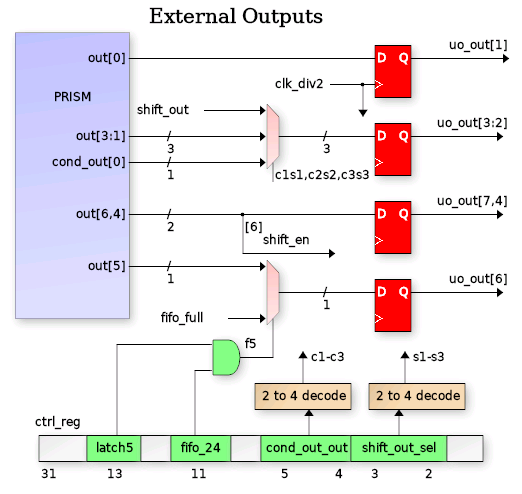
| output | name | effect |
|---|---|---|
| 0-3 | pin_out[3:0] | pin values, routed to uo_out[7:1] by PINMUX |
| 4 | OUT_LATCH | capture the in_prev flops, latched_in or the FSM flags |
| 5 | OUT_FIFO_WR_RD | push comm into an RX FIFO / pop a TX FIFO into comm (direction CFG0[23]) |
| 6 | OUT_COUNT1_INC_DEC | step count1, direction CFG0[14] |
| 7 | OUT_COUNT1_CLEAR_LOAD | clear count1, or load it from PRELOAD (CFG0[6]) |
| 8 | OUT_SHIFT | shift the selected shifter (CFG0[10]: comm or count1) |
| 9, 10, 11 | OUT_COUNT2_INC / DEC / CLEAR | count2 |
| 12 | OUT_CRC_CLEAR | preset the CRC (counter mode: preset the count) |
| 13 | OUT_CRC_UPDATE | feed the shifter's current bit into the CRC (counter mode: + 1) |
| 14 | OUT_HOST_INTERRUPT | raise the shard's interrupt, once per assertion |
| 15 | OUT_SEMA_CLEAR / OUT_FIFO_PUSH_POP | fractured: clear the semaphore; unfractured shard 0: output 5 acts on FIFO A (0) or FIFO B (1) |
| 16 | OUT_COMM_LOAD | load comm from PRELOAD[7:0], a constant K (CFG0[30]) or the constant table |
| 17 | OUT_LOAD_CRC | load the selected shifter from the CRC, one byte per load through comm (counter mode: - 1) |
| 18, 20 | OUT_K_SEL0 / 1 | which constant OUT_COMM_LOAD takes, or the table's index step; in multi-bit shift mode the width - 1 |
| 19 | OUT_SEMA_SET / OUT_FLAG2 | fractured: set the other shard's semaphore; with CFG0[29] the value OUT_LATCH stores in flag2 |
Each pin of uo_out[7:1] has a 3-bit PINMUX field: 0-3 the shard's pin_out[n], 4 and 5 its conditional outputs, 6 the shifter's serial bit (or a lane of the comm window in multi-bit mode), 7 not driven by this shard.
6. The datapath
Each shard has its own copy (prism_datapath.v), driven by its own outputs
and configured by its CFG0 (the chroma's ctrl_reg).
count1 is a 24-bit register, 32 bits with CFG0[11], that is either a counter or the wide shift register. As a counter it steps on output 6, down by default or up with CFG0[14]; output 7 clears it or loads it from PRELOAD (CFG0[6]); count1_term (input 10) marks zero counting down, or the preload (CFG0[15]) or the natural roll-over (input 23, count1_wrap) counting up; the host reads the count at +0x0C and a write loads it. As the wide shifter (CFG0[10]) it shifts on output 8, MSB or LSB first (CFG0[9]), taking its input from the pin CFG0[1:0] names, from cond_out[0] (CFG0[28]: a bit the FSM decoded, NRZI or Manchester) or from the Manchester recoverer; a load can count as the first bit already shifted (CFG0[16]) so shift_term marks the last. OUT_LOAD_CRC can load all 32 bits from the CRC.
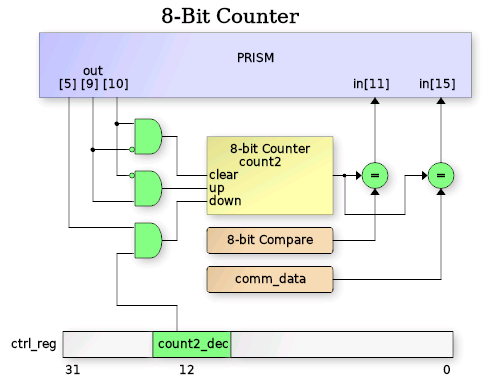
count2 is an 8-bit up / down / clear counter (outputs 9-11; the decrement is enabled by CFG0[12]) compared against the COMPARE byte (input 11, count2 >= COMPARE) and against comm (input 15, equality).
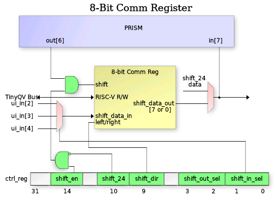
comm is the 8-bit communication shifter: it shifts on output 8 when CFG0[10] selects it, MSB or LSB first, from the same input choices as count1; it is what the FIFOs push and pop, what OUT_COMM_LOAD fills, and what OUT_LOAD_CRC loads one CRC byte at a time. A 3-bit shift count marks the byte boundary on shift_term, and a load or a FIFO pop can count as the first bit (CFG0[17]). With CFG0[2] (multi-bit shift) each OUT_SHIFT moves {OUT_K_SEL1, OUT_K_SEL0} + 1 bits at once from pins CFG0[1:0] .. + 3, and COMM_PINS (+0x50) names a 4-bit window of comm and a lane of it for every output pin, so a byte plays out as four bit pairs or two nibbles, PIO style; the shift count advances by the width so shift_term still marks the byte.
Constants: CONST (+0x38) holds K0..K3; with CFG0[30] OUT_COMM_LOAD loads K[{OUT_K_SEL1, OUT_K_SEL0}] (sync words, handshake codes), and K3 is also the byte comm is compared with for slot code 13. Constant table: when a shard runs on its SRAM FIFO the 64-byte latch FIFO's first 16 rows become an indexed table (CONST_TAB, +0x4C): OUT_COMM_LOAD loads the row at a 4-bit index, and the two K-select outputs say how the index moves on each load (clear, + 1, + add_to_idx, load idx_load), pre or post; a MAC address or a fixed reply costs no states.
Latches and flags: OUT_LATCH stores {shift_data, cond_out[0]} in latched_in (inputs 12-13); with CFG0[7] those inputs show two latched outputs instead; with CFG0[29] OUT_LATCH stores {cond_out[1], cond_out[0]} there and output 19 in flag2 (slot code 14), three flags a chroma sets and tests. CFG3[28] lets flag2 swap the sampler's edge.
The host sees the datapath in COUNTS (+0x10: count2, COMPARE, comm, and the shift counts) and FLAGS (+0x18: count1_term, count1_wrap, count2_cmp, count2 == comm, shift_term, shift_data, latched_in, FIFO empty and full, crc_ok, sampler edge pending).
7. Timers
count1 in counter mode is the general timer: load it from PRELOAD, count down, watch input 10.
Timer 2 (PRELOAD2, +0x40) is a free-running 24-bit timer with no FSM output: it reloads itself and raises input 28 for one clock every period + 1 clocks (0 = off), pacing things while count1 is busy (Ethernet link pulses every 16 ms need no CPU). With PRELOAD2[24] the count restarts whenever the shard enters state PRELOAD2[29:25], which makes the tick a retriggerable timeout ("nothing for N clocks since the last entry into RX_BIT") with no STEW bits; with [30] as well it ticks once per timeout and waits for the next entry.
8. FIFOs
Each shard has a 64-byte FIFO built from latch rows. CFG0[23] sets its direction: RX (0), the FSM pushes comm with output 5 and the host pops by reading +0x20; TX (1), the host pushes by writing +0x20 and output 5 pops the head into comm. A push on full and a pop on empty are ignored. FIFO_STATUS (+0x24) reads the count and the flags, and any write flushes. The almost-empty and almost-full levels are CFG1[19:16] / [23:20] in 4-byte units (almost-empty when count <= 4 x level, almost-full when count >= 64 - 4 x level); inputs 20 and 21 show two of the four flags, chosen by CFG1[27:24]. Contents survive PRISM disable, so a TX FIFO can be filled before the machine starts.
Two FIFOs for one machine: unfractured, shard 0 owns both FIFOs, A its own and B shard 1's (configured and served by the host through the shard 1 window). Output 15 says which one output 5 strobes, each per its own direction, so with A = RX and B = TX output 15 reads as "push / pop", and inputs 26-27 show B's flags. Single-FIFO chromas (output 15 = 0) behave as before.
SRAM FIFOs: with CFG0[31] a shard's FIFO is a 2 KB FIFO on its own IHP
512x32 SRAM macro (prism_sram_fifo.v), four bytes per word with a cached
head word, the same push / pop / flags interface, the count field widened,
and the levels in 64-byte units. An Ethernet receiver in one shard and a
transmitter in the other each get a full-frame buffer; unfractured, shard 0
reaches shard 1's SRAM as FIFO B.
32-bit access (CFG3[11], FIFO32 at +0x54): the host moves words. TX: a word written there is pushed a byte at a time, low byte first, one every fourth clock, waiting on a full FIFO; FIFO_STATUS[5] is busy meanwhile and a word written while busy is dropped, so poll it when the FIFO may be full (straight-line code never sees it: four pushes take 13 clocks, TinyQV's instructions 16). RX: a pop machine takes four bytes as soon as the FIFO holds them, low byte first, into a word register; FIFO_STATUS[4] and the shard's interrupt say the word is complete, and a read of FIFO32 takes it. A byte read of +0x20 while the word register holds anything is served from its low byte, the rest shift down and the machine refills the top, so byte order is the same however word and byte reads are mixed; a short message's stragglers show in FIFO_STATUS (the count, or [7:6] after byte reads) and are read as bytes.
9. CRC unit and counter mode
A bit-serial CRC per shard (prism_crc.v): width from CFG0[21:20] (8, 16
or 32 bits; 0 = off), a programmable polynomial (CRC_POLY, +0x28), reflected
(LSB first, CFG0[22]) or not, preset to zero or all ones (CFG0[25]) by
output 12, fed one bit per output 13 with the bit the shifter is receiving
or transmitting that clock (CFG0[27]), complemented on output (CFG0[26]).
The host reads or presets the value at +0x2C; input 22 (crc_ok, also
FLAGS[10]) says the value equals CRC_EXPECTED (+0x30), the residue after
data plus checksum, so a receiver checks a frame with one input. To
transmit a checksum, output 17 loads the selected shifter from the CRC: the
wide shifter takes all 32 bits, comm takes one byte per load in wire order
and the register advances, so CRC16 / CRC32 go out in 2 / 4 loads. CRC-8
0x07, CRC-16/CCITT 0x1021, CRC-16/USB 0xA001 (reflected), USB CRC5 0x14,
CRC-32 0xEDB88320 (reflected, Ethernet) have all run.
Counter mode (CFG3[10], with the CRC off): the same 32-bit register is an up / down counter on the same strobes, output 12 presets it, 13 counts up, 17 counts down (both in one cycle: hold; no shifter load), and input 22 becomes the unsigned compare count >= CRC_EXPECTED. The host reads or presets the count at +0x2C and sets the compare at +0x30. One adder and one comparator per shard; no extra flops.
10. Receiving clocked and self-clocked lines
Manchester bit recoverer (prism_mrx.v, CFG3[9:0]): names a pin
([2:0]), the clocks per half bit ([7:4]) and an enable ([3]); an edge on the
line is accepted when three quarters of a bit have passed since the last
accepted edge, so the boundary transition between equal bits is skipped
and every mid-bit edge re-times the decoder; the level after the accepted
edge is the bit. With [8] the shifter takes that bit as its input, and
"bit valid" is slot code 15, sticky until the FSM's shift consumes it, so a
two-state receive loop never misses a bit. With [9] the pin is sampled on
both clock edges and [7:4] counts half clocks per half bit (6 at 64 MHz, 5
at 50 MHz), doubling the edge resolution; 10BASE-T receive keeps its margin
down to a 50 MHz tile clock.
Edge-clocked sampler (CFG3[28:16]): names any PRISM input ([21:17]) and an edge ([23:22]: rising, falling, either), and on every such edge the datapath acts with no state transition: shift ([24]), count2 + 1 ([25]), capture the in_prev flops ([26]), count1 clear / load ([27]). A clocked slave protocol no longer spends states on its bit loop; the FSM acts at byte boundaries on shift_term or count2. With [28] flag2 swaps rising and falling, so one FSM flag turns a bidirectional protocol's sampling edge (an I2C target receives on SCL rising and drives after SCL falling). A sticky "edge pending" flag (slot code 15, FLAGS[11]) is cleared by the FSM's OUT_SHIFT or OUT_LATCH.
11. Interrupts
Each shard has one interrupt line to the host (TinyQV user interrupts 8 and 9, CTRL[31] and [29], INT_STATUS[1:0]). It is set by output 14 once per assertion (a state that holds it does not re-arm it), by a debugger halt, and in 32-bit RX mode while a complete word waits in FIFO32. It is cleared by a byte write with bit 7 to 0x003 (shard 0) or 0x007 (shard 1), by the host_in toggle write (+0x15), or by disabling PRISM; the word-ready source clears when the word is read.
12. Debugger
Each shard has a debug control word (0x04 shard 0, 0x08 shard 1):
| bits | field | meaning |
|---|---|---|
| 0 | halt_req | halt (on the rising edge) and hold |
| 1 | step | rising edge: execute one transition |
| 2, 3 | bp_en0, bp_en1 | breakpoint enables |
| 8:4, 13:9 | bp_si0, bp_si1 | breakpoint state |
| 15:14, 17:16 | bp_cond0, bp_cond1 | 0 on entry, 1 when tree 0 matches in the state, 2 when tree 1 is taken, 3 when either is, that is on exit |
| 18 | new_si | write-only: load the state index from bits 23:19 |
A conditional breakpoint fires in the cycle the selected tree first matches while the machine sits in the state, before the transition's outputs happen, so the value that satisfied the condition is still there to read; a single step then performs the transition with its outputs and halts in the target. Keep halt_req set while stepping. STATUS (0x0C) shows, per shard, the current and next state index, the halt and which breakpoint hit; 0x10-0x1C read back the four words of shard 0's current STEW; 0x34 the decision inputs and LUT results; 0x38 the outputs; 0x3C the input vector. While a shard is halted its datapath, pins, semaphores and interrupt edge are frozen with it.
13. Trace
Each shard has a tracer (TRACE_CFG +0x44, TRACE_CTRL +0x48). From its
trigger on, every clock's {executing, tree 1 taken, tree 0 matched, the six selected input bits, SI} is written as a 16-bit entry, two per SRAM
word, into an SRAM until the buffer is full: 1024 entries on one SRAM,
2048 with both as one buffer (TRACE_CFG[1]), and with TRACE_CFG[6] into the
other shard's SRAM so a chroma streaming from its own SRAM FIFO can be
traced while it does so. Triggers: at once; in a given state; that state
taking either jump; or an edge (rising, falling, either) on any of the 32
inputs. Entry 0 is the trigger cycle. Arm with TRACE_CTRL = 1 (the traced
SRAM's FIFO is flushed), wait for done (or stop with 2), then read the
entries as FIFO bytes through the window that reads that SRAM: while an
SRAM holds a finished trace the window sees it as its SRAM FIFO in RX mode,
count = entries x 2, each read of +0x20 the next byte, low byte first. The
21 outputs of a traced clock are not stored: they follow from the entry and
the loaded chroma (the STEW's three output fields), and the SDK rebuilds
them. One shard traces at a time; shard 0 wins if both enable.
14. CFGMEM: the state table and how it is loaded
The table is eight latch-array macros, 16 rows x 32 bits each, generated by
a DFFRAM-derived flow (CFGMEM_IHP16 and its left-hand mirror
CFGMEM_IHP_LEFT16; the views are in macros/), placed as two columns
beside the standard cells. Four macros make bank A (states 0-15: row s of
macros lo0..lo3 is state s's STEW, lo0 the low word) and four bank B
(hi0..hi3, states 16-31). Every clock the machine reads a whole 128-bit row
from each bank through the macros' read ports; latch arrays rather than
flops because a row is read every clock and written only when a chroma is
loaded, and a latch bit is far smaller than a flop with its write mux.
The CPU loads them through the CFGMEM loader peripheral at 0x8000100. Its
control byte at 0x1F is [3:0] row address, [4] address select (the host
addresses the row instead of the machine), [5] busy (read-only: the
loader's shift takes 49 clocks, more than a back-to-back store), [6]
bypass lo, [7] bypass hi. The four macros of a bank form a shift chain,
host word -> macro 0 -> 1 -> 2 -> 3, and each macro's output is its
addressed row, or its input while the bank's bypass bit is set. Loading is
therefore: set the bank's bypass bit, then for each state from the highest
down, write its four words, most significant first, to the macro ports
(0x00 + 4i for lo i, 0x20 + 4i for hi i, word 0 to macro 3 down to word
3 to macro 0), waiting on busy between writes; each write shifts the chain
one row, so state 0 ends in row 0. Clear the control byte afterwards to
hand the row address back to the machine. Reads with the bypass clear and
address select set return each macro's row at the addressed index, which
is how a loaded table is verified. The compiler's .py / .c output is
the word list in this order, so prism_load_chroma() is a loop.
15. Register map
All registers are word aligned at +4 offsets; a byte read returns the addressed byte lane in the low bits, so packed registers can be read and written a byte at a time. Offsets are from 0x8000200.
15.1 Common block
| offset | register |
|---|---|
| 0x00 | CTRL: [30] enable, [31] shard 0 interrupt (RO), [29] shard 1 interrupt (RO); byte 0x03 write with bit 7 clears shard 0's interrupt, byte 0x07 shard 1's |
| 0x04, 0x08 | DBG_CTRL shard 0 / shard 1 (section 12); read back = {state index[23:19], control[17:0]} |
| 0x0C | STATUS: shard 0 in [12:0], shard 1 in [25:13], each {break[1:0], halt, next SI[4:0], current SI[4:0]} |
| 0x10-0x1C | the four words of shard 0's current STEW |
| 0x20 | ID |
| 0x24 | INT_STATUS: [1:0] shard interrupts, [3:2] semaphores as seen by shard 0 / shard 1 |
| 0x30 | DEBUG_DOUT: the outputs a halted shard presents |
| 0x34 | DECISION: LUT inputs and results |
| 0x38 | OUT_DATA: the live output vector |
| 0x3C | IN_DATA: shard 0's input vector |
| 0x40 | FRAC_CFG: [0] fractured |
| 0x44, 0x48 | shard 0 output mask, conditional-output mask (fractured) |
| 0x4C, 0x50 | shard 1 output mask, conditional-output mask |
15.2 Shard window (shard 0 at 0x100, shard 1 at 0x180)
| offset | register |
|---|---|
| +0x00 | CFG0: datapath configuration, the chroma's ctrl_reg (section 15.3) |
| +0x04 | PINMUX: uo_out[7:1] sources, 3 bits per pin, the chroma's pinmux_reg |
| +0x08 | PRELOAD (32 bits) |
| +0x0C | COUNT1: read the count, write loads it |
| +0x10 | COUNTS: byte 0 count2, byte 1 COMPARE, byte 2 comm, byte 3 {comm_count[2:0], shift_count[4:0]} (RO); bytes 0-2 writable |
| +0x14 | HOST: host_in[1:0]; a byte write to +0x15 toggles host_in[0] and clears the interrupt |
| +0x18 | FLAGS (RO): [0] count1_term, [1] count1_wrap, [2] count2_cmp, [3] count2 == comm, [4] shift_term, [5] shift_data, [7:6] latched_in, [8] FIFO empty, [9] FIFO full, [10] crc_ok / count >= compare, [11] sampler edge pending |
| +0x1C | CFG1: [15:0] in_prev sources, [19:16] / [23:20] FIFO almost-empty / almost-full levels, [25:24] / [27:26] input 20 / 21 flag selects, [29:28] / [31:30] inputs 26 / 27 (FIFO B) |
| +0x20 | FIFO: byte write pushes (TX), byte read pops (RX) |
| +0x24 | FIFO_STATUS: {count[21:8], word bytes[7:6], push busy[5], word full[4], almost_full[3], almost_empty[2], full[1], empty[0]}; any write flushes |
| +0x28 | CRC_POLY |
| +0x2C | CRC: value; write presets (counter mode: the count) |
| +0x30 | CRC_EXPECTED (counter mode: the compare value) |
| +0x34 | CFG2: input slot selects, 4 bits each, inputs 16-19 in [15:0] and 28-31 in [31:16] |
| +0x38 | CONST: K0 [7:0] .. K3 [31:24] |
| +0x3C | CFG3: Manchester recoverer [9:0], counter mode [10], 32-bit FIFO access [11], edge-clocked sampler [28:16] |
| +0x40 | PRELOAD2: timer 2 [23:0] period, [24] restart on entry into state [29:25], [30] one-shot |
| +0x44 | TRACE_CFG (write-only): [0] enable, [1] both SRAMs, [6] other shard's SRAM, [3:2] trigger (0 now, 1 in state [12:8], 2 that state jumping, 3 an edge on input [20:16], [5:4] 0 rising 1 falling 2 either) |
| +0x48 | TRACE_CTRL: write [0] arm, [1] stop; read [0] armed, [1] running, [2] done, [3] big, [4] active |
| +0x4C | CONST_TAB: [0] enable, [1] add idx_load, [2] post, [7:4] idx_load, [10:8] add_to_idx, [19:16] index |
| +0x50 | COMM_PINS: [2:0] window base, [2k+5:2k+4] lane for uo_out[k+1] |
| +0x54 | FIFO32: 32-bit FIFO access (section 8) |
15.3 CFG0, the chroma's control word
| bits | name | meaning |
|---|---|---|
| 1:0 | shift_in_sel | the ui_in pin that feeds the shifter (multi-bit mode: pins sel .. sel + 3) |
| 2 | mshift_en | multi-bit comm shift, {out20, out18} + 1 bits per shift |
| 6 | clr_not_load | output 7 clears count1 instead of loading it |
| 7 | latch_in_out | inputs 13:12 show latched outputs instead of latched inputs |
| 8 | shift_en | shifting enabled |
| 9 | shift_dir | 0 MSB first, 1 LSB first |
| 10 | shift_wide | output 8 shifts count1 (1) or comm (0) |
| 11 | count32 | count1 is 32 bits (0: 24) |
| 12 | count2_dec_en | output 10 decrements count2 |
| 13 | latch_en | OUT_LATCH enabled |
| 14 | count_up | count1 counts up |
| 15 | wrap_preload | counting up rolls over at PRELOAD instead of naturally |
| 16 | shift_load_one | a wide-shifter load counts as the first shift |
| 17 | comm_load_one | a comm load or pop counts as the first shift |
| 19:18 | in_sync_sel | pin synchroniser: 0 two flops, 1 one flop, 2 raw |
| 21:20 | crc_mode | 0 off, 1 CRC-8, 2 CRC-16, 3 CRC-32 |
| 22 | crc_reflect | LSB first into the CRC |
| 23 | fifo_dir | 0 RX (FSM pushes, host pops), 1 TX (host pushes, FSM pops) |
| 24 | sema_set_wins | semaphore set beats clear in the same cycle |
| 25 | crc_init_ones | preset to all ones |
| 26 | crc_xor_out | complement on OUT_LOAD_CRC |
| 27 | crc_src | 0 the shifter's input bit, 1 its output bit |
| 28 | shift_in_cond | the shifter's input is cond_out[0] |
| 29 | flag_latch | OUT_LATCH stores {cond_out[1], cond_out[0]} in latched_in and output 19 in flag2 |
| 30 | comm_load_k | OUT_COMM_LOAD takes constant K[{out20, out18}] |
| 31 | fifo_sram | this shard's FIFO is its SRAM FIFO |
16. Chromas
A chroma is a Verilog module with the fixed ports clk, rst_n, fsm_enable, in_data[31:0], out_data[20:0], cond_out[1:0], ctrl_reg[31:0], pinmux_reg[20:0]: a state register, a case on it, if / else if / else
transitions on the inputs, and constant assignments to the outputs in each
state. The compiler is a Yosys backend
(yosys-prism, synth_prism -cfg chromas/tinyqv32.cfg): it maps the FSM onto the STEW fields, checks that
each state's conditions fit the six muxes and two trees, emits the inc
loop idiom, and writes the table as a Python list, a C array and a
columnar listing, together with the ctrl_reg and pinmux_reg values the
chroma declared. Rules it enforces: one wire per output bit, constants in
the always block (an input-dependent conditional output is written as a
default plus an if), and a trailing else -> next state behind at least
one condition always compiles to the auto-loop.
module chroma_uart_tx ( input clk, rst_n, fsm_enable, input [31:0] in_data,
                        output [20:0] out_data, output reg [1:0] cond_out,
                        output reg [31:0] ctrl_reg, output reg [20:0] pinmux_reg );
   ...
   STATE_IDLE:
      if (!fifo_empty)            // input 20
      begin
         fifo_pop = 1'b1;         // output 5: comm <= FIFO head
         count1_load = 1'b1;      // output 7: bit timer from PRELOAD
         next_state = STATE_START;
      end
   ...
The library in chromas/, every one with a cocotb test against a model of
the far end:
| chroma | what it does |
|---|---|
| gpio24 | 24-bit GPIO expander: 74165 in, 74595 out |
| spislave | SPI slave with a CRC-8 trailer |
| spi_master | SPI master, single or quad lane |
| uart_tx | 8N1 transmitter from the TX FIFO, CRC-8 on request |
| i2c_master | I2C controller through external open-drain buffers |
| i2c_slave | I2C target on the edge-clocked sampler |
| onewire | 1-Wire master |
| ws2812 | WS2812 LED transmitter |
| encoder | quadrature encoder decode |
| pio | 4-channel logic analyser and 2-lane waveform generator (multi-bit shift) |
| usb_ls | USB low-speed device: NRZI, bit unstuffing, CRC-5 / CRC-16, DATA0 / DATA1 |
| eth_tx | 10BASE-T transmitter from the SRAM FIFO, CRC-32 FCS, link pulses on timer 2 |
| eth_rx | 10BASE-T receiver on the Manchester recoverer, FCS checked by crc_ok |
| fifo_loop, edge, const_tab, counter | unit tests of the two-FIFO mode, the edge capture, the constant table and the counter mode |
The tests (test/user_peripherals/prism/) load each chroma through the
CFGMEM loader exactly as software does, and run unchanged on the gate-level
netlist. Host software uses prism.h from the
tinyQV-sdk with PRISM_CONFIG
janestreet: chroma loading, the datapath registers, FIFO and CRC access,
the sampler, the recoverer, timer 2, the constant table, the debugger and
the tracer, including the reconstruction of a trace's outputs.
The design record behind PRISM, decision by decision, is in prism_interface.md.
Pins
| Pin | Use |
|---|---|
| ui_in[6:0] | PRISM inputs 0-6 (each shard chooses raw, one-flop or two-flop synchronised) |
| ui_in[7] | TinyQV UART RX (or ui_in[3], by register) |
| uo_out[7:1] | PRISM outputs: each pin is routed by the running chroma to one of its four pin outputs, a conditional output or the shifter bit, or left to GPIO |
| uo_out[0] | TinyQV UART TX |
| uo_out[6] | doubles as the debug UART when selected |
| uio[7:0] | QSPI flash and PSRAM (bidirectional PMOD) |
TinyQV, the host processor
TinyQV is a small RISC-V CPU designed for Tiny Tapeout. It implements the
RV32EC instruction set plus the Zcb and Zicond extensions, with a couple of
caveats: addresses are 28 bits, program addresses 24 bits, and gp / tp
are hardcoded to 0x1000400 / 0x8000000. Instructions are read over QSPI
from flash and a QSPI PSRAM holds data; the two share the QSPI clock and
data lines, so only one is accessed at a time. Code runs from flash only.
In this design its job is to be PRISM's host: load a chroma, program the
datapath, feed and drain the FIFOs, service the interrupts.
TinyQV Memory map (host view)
| Address range | Device |
|---|---|
| 0x0000000 - 0x0FFFFFF | Flash |
| 0x1000000 - 0x17FFFFF | RAM A |
| 0x1800000 - 0x1FFFFFF | RAM B |
| 0x8000000 - 0x800003F | TinyQV debug and time |
| 0x8000040 - 0x800007F | GPIO |
| 0x8000080 - 0x80000FF | UART |
| 0x8000100 - 0x800013F | PRISM CFGMEM programming (state table loader) |
| 0x8000200 - 0x80003FF | PRISM: common block, shard 0 window at +0x100, shard 1 window at +0x180 |
| 0xFFFFF00 - 0xFFFFF07 | TIME |
PRISM's two shard interrupts are TinyQV user interrupts 8 and 9.
DEBUG
| Register | Address | Description |
|---|---|---|
| SEL | 0x800000C (R/W) | Bits 6-7 enable peripheral output on out6-7, otherwise out6-7 carry debug signals |
| DEBUG_UART_DATA | 0x8000018 (W) | Transmits the byte on the debug UART |
| STATUS | 0x800001C (R) | Bit 0: debug UART TX busy |
See also debug docs.
TIME
| Register | Address | Description |
|---|---|---|
| MTIME | 0xFFFFF00 (RW) | Get/set the 1 MHz time count |
| MTIMECMP | 0xFFFFF04 (RW) | Get/set the time to trigger the timer interrupt |
A 32-bit timer in the spirit of the RISC-V timer: MTIME advances at 1/64 of the clock (nominally 1 MHz) and the interrupt asserts while MTIME is past MTIMECMP by less than 2^30 microseconds.
GPIO
| Register | Address | Description |
|---|---|---|
| OUT | 0x8000040 (RW) | out0-7 when the GPIO function is selected |
| IN | 0x8000044 (R) | The current state of in0-7 |
| FUNC_SEL | 0x8000060 - 0x800007F (RW) | Function select for out0-7 |
| Function Select | Peripheral |
|---|---|
| 0 | Disabled |
| 1 | GPIO |
| 2 | UART |
| 8 | PRISM (a pin PRISM does not claim falls back to GPIO) |
UART
| Register | Address | Description |
|---|---|---|
| TX_DATA | 0x8000080 (W) | Transmits the byte |
| RX_DATA | 0x8000080 (R) | Reads any received byte |
| TX_BUSY | 0x8000084 (R) | Bit 0: TX busy; bit 1: a received byte is available |
| DIVIDER | 0x8000088 (R/W) | 13-bit clock divider for the baud rate |
| RX_SELECT | 0x800008C (R/W) | UART RX pin: ui_in[7] when 0 (default), ui_in[3] when 1 |
How to test
Bring-up is TinyQV's: load a program image into flash, reset (rst_n high
then low so the design sees a falling edge; program the flash and leave it in
continuous read mode and the PSRAMs in QPI mode; drive the QSPI chip selects
high with SD1:SD0 set to the read latency in cycles, 2 at 64 MHz; clock at
least 8 times and stop with the clock high; release the QSPI lines; raise
rst_n; then clock normally). The RP2040 on the Tiny Tapeout demo board does
this from MicroPython. Build programs with the
customised toolchain
and the tinyQV-sdk, whose prism.h
knows this tile's register map (PRISM_CONFIG janestreet).
A protocol is then a chroma, a Verilog Mealy state machine compiled by the yosys-prism backend into the 32 x 128-bit state table plus the datapath configuration words. The sequence, in software or from the test bench:
- Write the chroma from
chromas/, or take one of the seventeen there:makein that directory compiles them all (make yosysfetches and builds the compiler first). - Load the table through the CFGMEM loader (
prism_load_chroma()in the SDK: one word write per row with the bank's bypass bit set), program the shard's CFG0 / PINMUX from the compiler's output, set the datapath registers the chroma needs (preload, compare, constants, FIFO direction and levels), and set the enable bit. The machine starts in state 0. - Talk to it through the shard window: host_in bits for handshakes, the FIFO for data, the interrupt for completion, the debugger to halt, step and break, the tracer to record what it did.
The test suite is the reference for all of this: make -C test runs the
cocotb tests (test/user_peripherals/prism/), each a
chroma driven by a model of the device on the other side of the wire: the
GPIO expander, SPI slave and master, UART, I2C master and slave, 1-Wire,
WS2812, the quadrature encoder, the PIO logic analyser and generator, a USB
low-speed host talking to the device chroma; plus the fractured mode, the
FIFOs and their 32-bit access, the second timer, the sampler, the counter
mode and the debugger. The Ethernet, SRAM FIFO, constant table and tracer
tests skip on this tile. The same suite runs on the gate-level netlist.
External hardware
The design expects the QSPI PMOD on the bidirectional PMOD (16 MB flash, two 8 MB RAMs); the UART is on the pins of the demo board's RP2040 hardware UART.
Beyond that, whatever the protocol needs: PRISM drives logic levels on uo_out and reads them on ui_in. A USB low-speed device wants the usual series resistors and a 1.5 kOhm pull-up on D-, with D+ / D- on two outputs and an output-enable pin driving an external tri-state buffer. 10BASE-T (on the 8x4 tile) wants magnetics with a differential driver on the transmit pair and a receiver on the receive pair. I2C wants external open-drain buffers, since the tile's outputs are push-pull. Buttons on the inputs are handy for the host-in handshakes while developing.
IO
| # | Input | Output | Bidirectional |
|---|---|---|---|
| 0 | Interrupt 0 | UART TX | Flash CS |
| 1 | Interrupt 1 | SD0 | |
| 2 | SD1 | ||
| 3 | SCK | ||
| 4 | SD2 | ||
| 5 | SD3 | ||
| 6 | Debug UART TX | RAM A CS | |
| 7 | UART RX | Debug signal / PWM | RAM B CS / PWM |