548 Circuitli C061618G2TR
548 : Circuitli C061618G2TR
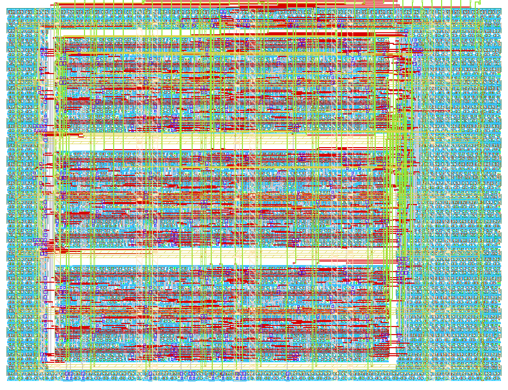
- Author: circuitli
- Description: A triple redundant clockless MMU module with an integrated anti-glitch filter network for 8-bit processors with a 16-bit address bus.
- GitHub repository
- Open in 3D viewer
- Open in Tiny Tapeout Explorer
- Clock: 0 Hz
How it works
This project is a Memory Management Unit (MMU). It handles memory mapping, peripheral address decoding, and operating system banking across the computer's memory map.
- Address Decoding: The circuit accepts high-order CPU address lines (A11 to A15) alongside primary system configuration flags to determine which physical hardware target should be active during a memory read/write cycle.
- Banking Logic & PORTB: It actively monitors control inputs. This includes decoding signals to dynamically switch the internal 16KB Operating System ROM, the BASIC ROM, and the Self-Test ROM in and out of the memory map, freeing up underlying DRAM when disabled.
- Peripheral Mapping: The internal combinatorial decoding grid maps out active-low chip select signals for custom sub-systems and the master RAM network.
This design acts as a purely combinatorial logic array.
How to test
This project is currently validated using an automated simulation environment (Cocotb or HDL testbench). You can run the testbench and inspect the generated waveform file (VCD) using the following verification steps:
- Initialize Simulation: Run the test suite using `make test'.
- Verify Basic OS ROM Mapping:
- In the testbench stimulus, drive the address bus inputs
A[15:11]to5'b11111(representing memory space$F800-$FFFF). - Assert the
REN(ROM Enable) control input high. - Inspect the waveform viewer to verify that the OS Chip Select output (OS_L) and CI_L drop to 0.
- In the testbench stimulus, drive the address bus inputs
- Verify BASIC Banking Logic:
- Drive the address inputs to
5'b10101(representing memory space$A000-$BFFF). - Toggle the
BE_Lsimulation signal to 0. - Assert that BASIC_L falls to 0. Then, drive BE_L to 1 and verify the output switches back to exposing the underlying system memory by resetting CI_L` to 1.
- Drive the address inputs to
- I/O Device Matrix Test:
- Force the address lines to match the hex-equivalent binary for
$D300. - Check the simulation logs or waveform to confirm that only the IO_L output line drops to logic 0.
- Force the address lines to match the hex-equivalent binary for
External hardware
None for now.
IO
| # | Input | Output | Bidirectional |
|---|---|---|---|
| 0 | A11 | REN | S5_L |
| 1 | A12 | REF_L | BASIC_L |
| 2 | A13 | MPD_L | OS_L |
| 3 | A14 | BE_L | CI_L |
| 4 | A15 | IO_L | |
| 5 | MAP_L | TRIGGER_OUT_L | S4_L |
| 6 | RD4 | FLG_IN_L | FLG_L |
| 7 | RD5 |