356 Digital IQ Lock-in (IEEE)
356 : Digital IQ Lock-in (IEEE)
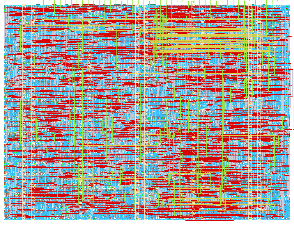
- Author: Gabriela Sheilyn Ticona Jimenez
- Description: Dual-phase digital demodulator with programmable block averaging — Equipo Triada CEG
- GitHub repository
- Open in 3D viewer
- Open in Tiny Tapeout Explorer
- Clock: 50000000 Hz
Digital IQ Lock-in Amplifier — TTIHP26b 1x1
Overview
This project implements a dual-phase digital lock-in amplifier / I/Q demodulator for the Tiny Tapeout IHP shuttle.
The design receives signed 8-bit input samples, generates internal quadrature reference signals, performs I/Q synchronous demodulation, and applies programmable block averaging.
This revision has been specifically optimized to improve the probability of fitting inside a single 1x1 IHP Tiny Tapeout tile.
The main design goals are:
- signed 8-bit input samples;
- digital I/Q demodulation;
- programmable 16-bit phase step;
- 32-point reference waveform;
- selectable averaging windows of 16, 64, 256, or 1024 samples;
- coherent 16-bit I/Q result readout;
- low-area RTL architecture suitable for a
1x1Tiny Tapeout allocation.
The project keeps:
tiles: "1x1"
in info.yaml.
A successful Tiny Tapeout GDS workflow is still required to confirm that placement, routing and timing physically fit inside the allocated 1x1 tile.
How it works
The system is divided into three main internal blocks:
reference_generatorlockin_coreregister_interface
The top-level module is:
tt_um_gstj_lockin
implemented in:
src/project.v
1. Reference generator
The reference_generator contains a 16-bit phase accumulator.
The phase is incremented only when the lock-in core actually accepts an input sample.
Conceptually:
phase = phase + phase_step
The programmable value phase_step therefore controls the frequency of the internally generated reference.
Only the five most significant bits of the phase accumulator are used to address the reference waveform:
phase_index = phase[15:11]
This produces:
2^5 = 32
possible phase positions.
The lower 11 bits are still preserved internally, so arbitrary 16-bit phase_step values retain fractional phase resolution.
The phase accumulator is reset to zero when the design is reset or when the active measurement configuration is changed.
2. I/Q demodulation
The lock-in amplifier performs two synchronous products for every accepted input sample.
Conceptually:
I = sample × cos(reference_phase)
Q = sample × -sin(reference_phase)
These products are accumulated over a programmable number of samples.
After the selected block has been completed, the accumulated values are divided by the block length.
The available averaging windows are:
window_sel |
Number of samples | Division |
|---|---|---|
00 |
16 | /16 |
01 |
64 | /64 |
10 |
256 | /256 |
11 |
1024 | /1024 |
The default value after reset is:
window_sel = 2
therefore the default averaging window is:
256 samples
3. Area-optimized architecture
The original RTL already requested a 1x1 tile, but declaring:
tiles: "1x1"
does not guarantee that the synthesized standard cells can physically fit inside that area.
For this reason, the datapath was redesigned specifically to reduce silicon area.
The most important changes are described below.
Serial multiplier
The previous architecture used a generic signed:
8 × 8 bit combinational multiplier
Although the multiplier was shared between the I and Q calculations, a combinational multiplier can still require a significant amount of standard-cell area.
The optimized architecture removes this multiplier.
Multiplication is now performed using a serial shift-and-add datapath.
The same arithmetic hardware is reused for I and Q.
Each reference coefficient has a maximum magnitude of 127, which requires seven magnitude bits.
Therefore one product requires approximately:
7 serial multiplication cycles
The datapath performs:
7 cycles for I
7 cycles for Q
instead of synthesizing a complete parallel 8x8 multiplier.
This deliberately exchanges throughput for lower silicon area.
4. Compact reference LUT
The reference waveform contains 32 phase positions.
The original implementation explicitly represented the complete sine waveform and evaluated sine/cosine references separately.
The optimized implementation exploits sine-wave symmetry.
Instead of storing all 32 signed values, only nine non-negative magnitudes are required:
| Index | Magnitude |
|---|---|
| 0 | 0 |
| 1 | 25 |
| 2 | 49 |
| 3 | 71 |
| 4 | 90 |
| 5 | 106 |
| 6 | 117 |
| 7 | 125 |
| 8 | 127 |
The other values are reconstructed using quarter-wave symmetry and sign inversion.
This produces the same 32-point numerical waveform while reducing duplicated lookup logic.
The same LUT hardware is reused sequentially for both quadrature references.
5. Reduced accumulator width
The original architecture used two signed 26-bit accumulators.
The optimized implementation uses:
25-bit signed accumulators
for both I and Q.
This reduction is mathematically safe.
The maximum magnitude of an input sample is:
128
because the signed 8-bit input range is:
-128 ... +127
The maximum reference magnitude is:
127
The largest averaging block contains:
1024 samples
Therefore the worst-case accumulated magnitude is:
1024 × 128 × 127
which gives:
16,646,144
A signed 25-bit value has the range:
-16,777,216 ... +16,777,215
Therefore 25 bits are sufficient to represent the complete worst-case accumulated value without saturation.
6. Fixed averaging shifts
The previous implementation calculated the average using a variable arithmetic right shift.
Conceptually:
sum >>> shift_count
where:
shift_count = 4, 6, 8 or 10
A variable shift can synthesize into a barrel-shifter or multiplexer network.
The optimized implementation instead uses fixed bit slices.
Conceptually:
/16   -> shift 4
/64   -> shift 6
/256  -> shift 8
/1024 -> shift 10
The required slice is selected according to window_sel.
The same averaging logic is reused sequentially for I and Q.
7. Result storage optimization
The previous architecture contained two copies of the I/Q result:
core result registers
+
register-interface snapshot registers
This duplicated approximately 32 bits of result storage.
The optimized architecture removes this duplication.
The completed results are written directly into the readback registers.
Internally each result is stored as a signed:
15-bit value
and is sign-extended when exposed through the 16-bit register interface.
The average of a signed 8-bit sample multiplied by a reference whose magnitude is at most 127 fits safely inside this range.
8. SNAPSHOT_STROBE behavior
Because the readback registers now directly contain the latest complete result, copying the result into another snapshot register is no longer necessary.
For pin compatibility the signal is still called:
SNAPSHOT_STROBE
but its function is now an acknowledge signal.
When asserted, it clears:
NEW_RESULT
The I/Q values themselves remain stored.
Therefore the recommended sequence is:
wait for NEW_RESULT = 1
read I
read Q
pulse SNAPSHOT_STROBE
After the pulse:
NEW_RESULT = 0
but the previous result remains available in registers 0-3 until a new result is generated or the measurement state is cleared.
Pin interface
Dedicated input bus
ui_in[7:0]
is used as:
DATA_IN[7:0]
For sample acquisition it represents a signed 8-bit value:
-128 ... +127
During register writes the same bus contains the register data.
Dedicated output bus
uo_out[7:0]
is:
READ_DATA[7:0]
The value depends on the register selected with ADDR[2:0].
Bidirectional pins
| Pin | Signal | Direction |
|---|---|---|
uio[0] |
SAMPLE_STROBE |
Input |
uio[1] |
WRITE_STROBE |
Input |
uio[2] |
ADDR[0] |
Input |
uio[3] |
ADDR[1] |
Input |
uio[4] |
ADDR[2] |
Input |
uio[5] |
SNAPSHOT_STROBE / ACK |
Input |
uio[6] |
BUSY |
Output |
uio[7] |
NEW_RESULT |
Output |
The output-enable configuration is:
uio_oe = 8'b11000000;
Therefore only:
uio[6]
uio[7]
are driven by the ASIC.
Register map
The register address is selected using:
uio_in[4:2]
giving eight addresses.
| Address | Read | Write |
|---|---|---|
0 |
I result, bits 7:0 | — |
1 |
I result, bits 15:8 | — |
2 |
Q result, bits 7:0 | — |
3 |
Q result, bits 15:8 | — |
4 |
phase_step[7:0] |
phase_step[7:0] |
5 |
phase_step[15:8] |
phase_step[15:8] |
6 |
window_sel |
window_sel |
7 |
Status | Control |
Phase-step configuration
The reference phase increment is a 16-bit value.
The low byte is located at:
register 4
and the high byte at:
register 5
Therefore:
phase_step = {register_5, register_4}
The default reset value is:
0x1000
Writing either phase-step byte clears the current accumulation and restarts the reference phase.
This prevents measurements obtained using different reference configurations from being mixed in the same averaging block.
Averaging-window configuration
Register:
6
contains:
window_sel[1:0]
The mapping is:
00 -> 16 samples
01 -> 64 samples
10 -> 256 samples
11 -> 1024 samples
Writing this register clears the current accumulation and restarts the reference phase.
Status register
Register:
7
returns:
{5'b00000, OVERRUN, NEW_RESULT, BUSY}
Therefore:
| Bit | Signal |
|---|---|
| 0 | BUSY |
| 1 | NEW_RESULT |
| 2 | OVERRUN |
| 7:3 | Reserved / 0 |
BUSY
BUSY indicates that the arithmetic datapath is currently processing a sample.
A new sample should only be sent when:
BUSY = 0
The serial arithmetic engine spends approximately:
7 clocks -> I multiplication
7 clocks -> Q multiplication
for a normal sample.
The final sample of each averaging block additionally requires two cycles to output the completed I and Q averages.
Consequently the controller must always use the BUSY handshake rather than assuming that a new sample can be accepted every clock cycle.
At the configured:
50 MHz
clock, the architecture is still capable of processing input samples on the order of several million samples per second while using considerably less combinational arithmetic hardware than the parallel-multiplier architecture.
NEW_RESULT
NEW_RESULT is asserted after a complete I/Q result pair has been generated.
The core outputs the I result first and the Q result afterward.
NEW_RESULT is asserted only after Q has been stored.
Therefore software never treats a partially updated I/Q pair as a complete measurement.
When:
NEW_RESULT = 1
registers 0-3 contain one coherent result pair.
OVERRUN
OVERRUN becomes active if a new sample request is generated while the arithmetic core is already busy.
Conceptually:
SAMPLE_STROBE while BUSY = 1
causes:
OVERRUN = 1
The flag is sticky until the system is cleared.
The controller should therefore always check:
BUSY = 0
before generating another SAMPLE_STROBE.
Feeding a sample
To submit a sample:
- Wait until:
BUSY = 0
- Place the signed 8-bit sample on:
ui_in[7:0]
- Pulse:
SAMPLE_STROBE
for one clock.
The interface performs rising-edge detection, so the strobe should return low before another sample request is generated.
When the sample is accepted, the phase accumulator advances exactly once.
Writing a register
To write configuration data:
- Put the register address on:
uio_in[4:2]
- Put the value on:
ui_in[7:0]
- Pulse:
WRITE_STROBE
for one clock.
Writes to registers:
4
5
6
automatically clear the current measurement accumulation.
Reading the I/Q result
Wait until:
NEW_RESULT = 1
Then read:
register 0 -> I[7:0]
register 1 -> I[15:8]

register 2 -> Q[7:0]
register 3 -> Q[15:8]
The high result byte is sign-extended from the internal signed result representation.
After the four bytes have been read, pulse:
SNAPSHOT_STROBE
to acknowledge the result.
This clears:
NEW_RESULT
without deleting the stored I/Q data.
Clear / restart control
Writing register 7 with bit 0 equal to one:
data_in[0] = 1
clears the active measurement state.
This resets:
I accumulator
Q accumulator
sample counter
stored I result
stored Q result
NEW_RESULT
OVERRUN
reference phase
The configured:
phase_step
window_sel
are preserved.
Enable behavior
The Tiny Tapeout ena signal enables operation of the internal datapath and register events.
If:
ena = 0
the design does not accept new arithmetic operations.
Area optimization summary
The principal area reductions are:
| Structure | Previous architecture | 1x1-optimized architecture |
|---|---|---|
| Multiplier | Signed combinational 8x8 multiplier | Shared serial shift/add multiplier |
| I/Q multiplication | Shared multiplier used sequentially | Single serial datapath reused for I and Q |
| Reference waveform | Complete LUT evaluations | Folded quarter-wave LUT |
| Stored magnitudes | Full 32-point waveform | 9 magnitudes |
| Accumulators | 26-bit I + 26-bit Q | 25-bit I + 25-bit Q |
| Averaging | Variable arithmetic shift | Fixed bit slices |
| Result registers | Core result + snapshot result | One readback result pair |
| Internal result width | 16 bits | 15 bits with sign extension |
| Placement density | 60% | 70% |
| Tile allocation | 1x1 | 1x1 |
Physical implementation configuration
The project uses:
CLOCK_PERIOD = 20 ns
corresponding to:
50 MHz
The optimized placement target is:
PL_TARGET_DENSITY_PCT = 70
The tile allocation remains:
tiles: "1x1"
The density value was increased from the previous 60% target so that the placer can use the limited 1x1 floorplan more efficiently.
Increasing placement density does not itself reduce synthesized cell area, which is why the RTL datapath was also redesigned.
Main optimization strategy
The design follows an area-first strategy:
parallel arithmetic
        ↓
serialized arithmetic

duplicated logic
        ↓
shared logic

duplicated registers
        ↓
single result storage

generic variable operations
        ↓
fixed operations

full waveform LUT
        ↓
symmetry-reduced LUT
The architecture therefore intentionally prioritizes:
small silicon area
over:
maximum sample throughput
which is appropriate for the 1x1 Tiny Tapeout target.
Verification
The verification environment uses Cocotb.
The tests compare the RTL output against an independent integer model of the digital lock-in amplifier.
The verification includes:
- reset behavior;
- phase-step programming;
- all four averaging windows;
- multiple phase steps;
- phase accumulator wrapping;
- signed input samples;
- I/Q result generation;
- noisy signal recovery;
- amplitude/phase behavior;
BUSYbehavior;NEW_RESULT;- overrun detection;
- enable gating;
- configuration changes;
- accumulation reset behavior.
The numerical 32-point reference waveform is preserved by the compact LUT architecture.
The serial multiplication architecture is intended to produce the same integer product as the previous parallel multiplication implementation.
Files used by the design
The relevant RTL files are:
src/project.v
src/reference_generator.v
src/lockin_core.v
src/register_interface.v
Physical implementation configuration:
src/config.json
Tiny Tapeout project configuration:
info.yaml
Verification:
test/test.py
test/tb.v
test/Makefile
Project documentation:
docs/info.md
External hardware
No external hardware is required for RTL simulation.
Simulation can provide signed 8-bit samples directly to the design.
For physical operation, an external controller must:
- supply signed 8-bit samples;
- generate
SAMPLE_STROBE; - wait for
BUSY; - configure the registers;
- detect
NEW_RESULT; - read the I/Q result registers.
If the input originates from an analog signal, external hardware is also required for:
ADC
signal conditioning
anti-alias filtering, if required
The ASIC design itself does not contain an ADC.
Final 1x1 verification
The project is structurally optimized for a Tiny Tapeout IHP:
1x1
tile.
However:
tiles: "1x1"
only defines the requested physical allocation.
It does not prove that synthesis, placement and routing will succeed.
The definitive verification is the Tiny Tapeout GitHub:
GDS
workflow.
The design should only be considered physically validated for 1x1 after the complete GDS flow passes successfully.
Important checks include:
synthesis
floorplanning
global placement
detailed placement
clock-tree synthesis
routing
timing
DRC / implementation checks
If global placement fails because of excessive utilization or congestion, the first step should be to inspect the synthesis and placement reports rather than immediately increasing the tile allocation.
The objective of this revision is to preserve:
tiles: "1x1"
and reduce the RTL area until the physical implementation successfully fits inside that allocation.
IO
| # | Input | Output | Bidirectional |
|---|---|---|---|
| 0 | DATA_IN[0] | READ_DATA[0] | SAMPLE_STROBE |
| 1 | DATA_IN[1] | READ_DATA[1] | WRITE_STROBE |
| 2 | DATA_IN[2] | READ_DATA[2] | ADDR[0] |
| 3 | DATA_IN[3] | READ_DATA[3] | ADDR[1] |
| 4 | DATA_IN[4] | READ_DATA[4] | ADDR[2] |
| 5 | DATA_IN[5] | READ_DATA[5] | SNAPSHOT_STROBE |
| 6 | DATA_IN[6] | READ_DATA[6] | BUSY |
| 7 | DATA_IN[7] | READ_DATA[7] | NEW_RESULT |