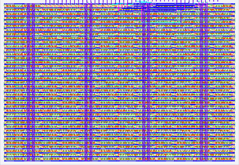
803 YoshiTP
803 : YoshiTP

- Author: Yeshua M (Yoshi)
- Description: Tiny Tapeout Microchip creates the letter M if flipped horizontally
- GitHub repository
- Open in 3D viewer
- View in Wokwi
- Clock: 0 Hz
How it works
This project is a tiny TDC constructed entirely of standard cells. During the Tapeout, we are creating a MOSFET. A MOSFET is a type of Transistor that can be used as a digital watch. The name stands for Metal Oxide Semiconductor Field Effect Transistor. When a voltage is applied across the gate and body, an electric field forms in the channel, attracting charge carriers to enable conduction. In an N-type MOSFET on a P-type substrate, minority carriers (electrons) form the conductive channel between the drain and the source. In a P-type MOSFET, the process is reversed: the substrate is N-type, and minority carriers (holes) create the channel. Since holes have lower mobility than electrons, P-type MOSFETs typically require a wider channel (2-3 times larger) than N-type MOSFETs for matching performance. To avoid increasing cell size, standard cells often don't match P and N strengths. Doping the silicon controls the ratio of charge carriers.
During the tape out when turning on or turning of the switches IN1-7 is causes a reaction on the lights that turn it on (OUT1-7).
How to test
To test the MOSFET you can switch on and off switches to cause a reaction on the "digital watch light"
External hardware
LED lights were used such as the Digital watch to view the numbers. (UNSURE) but the Logics "NAND Gate" and the "Not Gate" been used to create my initial of my last name
IO
| # | Input | Output | Bidirectional |
|---|---|---|---|
| 0 | IN0 | OUT0 | |
| 1 | IN1 | OUT1 | |
| 2 | IN2 | OUT2 | |
| 3 | IN3 | OUT3 | |
| 4 | IN4 | OUT4 | |
| 5 | IN5 | OUT5 | |
| 6 | IN6 | OUT6 | |
| 7 | IN7 | OUT7 |