265 tt_um_tim2305_adc_dac
265 : tt_um_tim2305_adc_dac

- Author: Timonas Juonys
- Description: 8bit dac and 4bit flash adc
- GitHub repository
- Open in 3D viewer
- Clock: 50000000 Hz
How it works
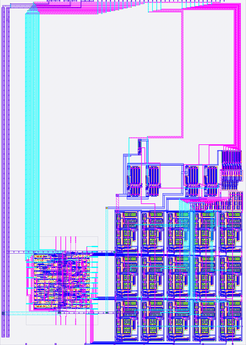
8 bit r2r dac inputs are connected directlly to the digital input pins. its output can be connected to the analog pin by setting the dac_connect pin high. the connection is made by a transmission gate. 4bit flash adc has an input range of 0-1 volts, it refference voltages are set by a resistive voltage divider. the upper bound (the top voltage) used by the divider can be connected to the analog pin for calibration by setting adc_cal_connect pin high. The output of the adc is multiplexed on 3 4 bit busses, this way the frequency on the digital outputs pins is 3 times lower than the clock.
How to test
to test the dac: set adc_connect = 1 and adc_cal_connect = 0 put your number on the 8 input pins and read the analog voltage
to test the adc just clock the design and read the bus pins. you can use the internal dac or you can disconnect the dac and connect an external voltage source.
External hardware
List external hardware used in your project (e.g. PMOD, LED display, etc), if any
IO
| # | Input | Output | Bidirectional |
|---|---|---|---|
| 0 | dac0 | bus0[0] | bus2[0] |
| 1 | dac1 | bus0[1] | bus2[1] |
| 2 | dac2 | bus0[2] | bus2[2] |
| 3 | dac3 | bus0[3] | bus2[3] |
| 4 | dac4 | bus1[0] | dac_conn |
| 5 | dac5 | bus1[1] | adc_cal_conn |
| 6 | dac6 | bus1[2] | sti_conn |
| 7 | dac7 | bus1[3] | sti_dac_conn |
Analog pins
ua | PCB Pin | Internal index | Description |
|---|---|---|---|
| 0 | B4 | 10 | a |