836 TT09 SKY130 ROM Test
836 : TT09 SKY130 ROM Test

- Author: Sylvain Munaut
- Description: Test of some prototype ROM macros
- GitHub repository
- Open in 3D viewer
- Clock: 0 Hz
How it works
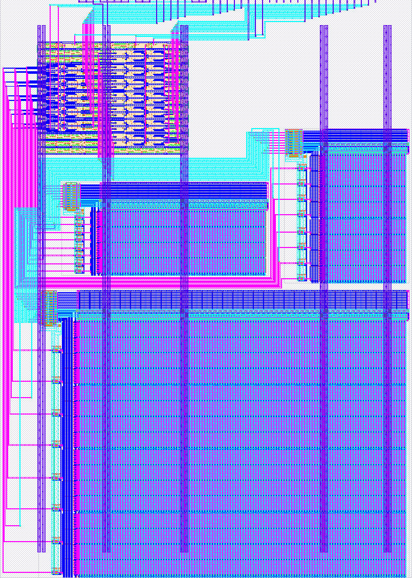
Just some registers in front of a few ROM macros to be able to send the address and capture data at specific intervals.
How to test
Set clk and rst_n to select one of the 4 possible testing
mode.
Load a test address to read setting half the bits on ui[6:0]
and then using both ui[7] and uio[7] to load the internal
preload register.
Then apply a clock edge on uio[6] to clock the address register
which will transfer the address from the pre-load register to the
actual address register and send the address to the ROMs.
After some delay, apply a clock edge on uio[5] which will capture
the output of the ROM.
External hardware
To do any meaningful timing testing you'll need some FPGA hardware to drive the various control signal in sequence with precise timings.
The exact testing platform is still TBD.
IO
| # | Input | Output | Bidirectional |
|---|---|---|---|
| 0 | addr_in[0] | data[0] | data[5] |
| 1 | addr_in[1] | data[1] | data[6] |
| 2 | addr_in[2] | data[2] | data[7] |
| 3 | addr_in[3] | data[3] | data[8] |
| 4 | addr_in[4] | data[4] | data[9] |
| 5 | addr_in[5] | clk of data register | |
| 6 | addr_in[6] | clk of addr register | |
| 7 | clk of addr_ld[13:7] register | clk of addr_ld[6:0] register |