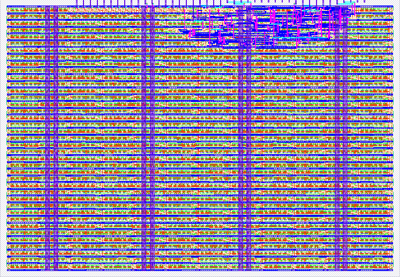
751 tt09-C6-array-multiplier
751 : tt09-C6-array-multiplier

- Author: Jonathan Farah and Josef Anurov
- Description: 4x4 multiplier
- GitHub repository
- Open in 3D viewer
- Clock: 0 Hz
How it works
4 x 4 Array Multiplier Circuit Diagram The circuit implements a 4 x 4 array multiplier using manual structural design. The array multiplier was created by using partial products and 4-bit adders. There are 2 inputs: m and q, which represent 4-bit input numbers to be multiplied. It outputs p, an 8-bit product of m and q. It has Wires w1,w2,w3 and w4. These represent the partial products generated from each bit of q multiplied by each bit of m. Wires: partial1, partial2, and partial3 store intermediate sums of partial products as they are added.
How to test
We test using some test numbers and checking the output. Wires C[2:0] are carry bits between the adders. Each w vector (from w1 to w4) represents the result of ANDing each bit of m with a specific bit of q. The add_4bit modules add these partial products together, simulating a ripple-carry addition for each shifted partial product. In terms of assigning the final product is constructed from the individual bits. The MSB comes from C[2]. Bits of partial3, partial2, partial1, and w1 make up the remaining bits, in that order. The implementation of the circuit was then tested using the provided Verilog testbench. The testbench was given a combination of inputs that effectively tested each case to ensure that the multiplier ran correctly.
External hardware
N/A
IO
| # | Input | Output | Bidirectional |
|---|---|---|---|
| 0 | q[0] | p[0] | |
| 1 | q[1] | p[1] | |
| 2 | q[2] | p[2] | |
| 3 | q[3] | p[3] | |
| 4 | m[0] | p[4] | |
| 5 | m[1] | p[5] | |
| 6 | m[2] | p[6] | |
| 7 | m[3] | p[7] |