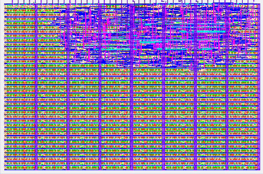
215 Clock synchronizer
215 : Clock synchronizer

- Author: Mateo Guerrero Gonzalo Hernandez Cesar Azambuya Francisco Veirano
- Description: Testing different ways of clock synchronizers to avoid metastability problems.
- GitHub repository
- Open in 3D viewer
- Clock: 10000000 Hz
How it works
This project is composed by different clock synchronizers subblocks. The function of these subblocks is to mitigate the problem of metastability caused when you have two clock domains and you want to transfer a signal from one domain to another. Then, with a selector input, you can select the output from the different subblocks in order to test and measure their performance to avoid this problem.
So, the project has: A first register at the input to hold the data. This 8 bits-length data is registered by CLK1.
This data is registered by another second register but with another clock, in this case CLK2. The data of the output of this register has a high probability to be metastable.
The output of the first register is the input of the three different blocks to be tested.
1- The first one, 2 flip-flop synchronizer, is composed by two register in cascade (A connected to B), triggered by CLK2. There is probability that while sampling the input A-d by flip flop A in CLK2 clock domain, output A-q may go into metastable state. But during the one clock cycle period of CLK2 clock, output A-q may settle to some stable value. Output of flop B can go to metastable if A does not settle to stable value during one clock cycle, but probability for B to be metastable for a complete destination clock cycle is very close to zero.
2- The second, Recirculation mux synchronization, in order to synchronize data, a control pulse is generated in source clock domain (CLK1) when data is available at source flop. Control Pulse is then synchronized using 2 flip flop synchronizer or pulse synchronizer (Toggle or Handshake) depending on clock ratio between source (CLK1) and destination (CLK2) domain. Synchronized control pulse is used to sample the data on the bus in destination domain. Data should be stable until it is sampled in destination clock domain (CLK2).
3- The third, Toggle block, is the same as Recirculation mux synchronization block, but in this case we generate the control pulse using a Toggle synchronizer. The toggle synchronizer is used to synchronize a pulse generating in source clock domain (CLK1) to destination clock domain (CLK2). A pulse cannot be synchronized directly using 2 FF synchronizer. While synchronizing from fast clock domain (CLk2) to slow clock domain (CLk1) using 2 FF synchronizer, the pulse can be skipped which can cause the loss of pulse detection and hence subsequent circuit which depends upon it, may not function properly.
The project also has enable control block. This block controls that the synchronizer subblocks run only once each, generating a pulse in their respective enable inputs.
How to test
First, you need to define the frequency you want to use with CLK1 and CLK2. After reset, you need to put an input data on data_in bus (uio_in). If you want to use de enable control block, you need to put enable_block input (ui_in[6]) at low level all the time, and rise a pulse of one period of CLK1 duration in trigger input (ui_in[7]). Otherwise, you can put enable_block in high level all the time. In this case, all blocks are going to be updating their values constantly. You will see at the output the signal and examine if the signal has a metastable state or not, switching between the diferent output using the sel input (ui_in[3:1]). Also, you can use the input stb and pulse_in to measure the performance of the blocks associated to these inputs. These signals are used as triggers to register data in CLK2 domain.
IO
| # | Input | Output | Bidirectional |
|---|---|---|---|
| 0 | clk, clock of the first clock domain. | data_out connected to uo_out. This is the data output of the different block depending of the value of sel. | data_in connected to uio_in, set as input. This is the data input to be synchronized. |
| 1 | clk_2 connected to ui_in[0]. This is the second clock domain. | When the input sel = 0 you will see the output of the first FF (triggered by CLK1). | |
| 2 | sel connected to ui_in[3:1]. This the selector tu select the different output between the different blocks. | When the input sel = 1 you will see the output of the second FF (triggered by CLK2). | |
| 3 | stb connected ui_in[4]. This is the pulse needed to synchronize with the second block. | When the input sel = 2 you will see the first block using to synchronize (triggered by CLK2). | |
| 4 | pulse_in connected to ui_in[5]. This is the pulse needed to synchronize with the third block. | When the input sel = 3 you will see the second block using to synchronize (triggered by CLK1 and CLK2). | |
| 5 | rst_n. Reset of the system. | When the input sel = 4 you will see the third block using to synchronize (triggered by CLK1 and CLK2). | |
| 6 | ena. Will go high when the design is enabled. | When the input sel = 5 you will see the output {stb_in, ctrl, stb_out, A, B1, B2, B3, pulse_out}, the intermediate signals of the different blocks. | |
| 7 | enable_block connected to ui_in[6]. This signal is used to enable all subblocks. | When the input sel = 6 you will see the output {0, 0, ena_A, ena_1, ena_2, ena_3, done} the enables of the different blocks. |