197 ROTFPGA v2
197 : ROTFPGA v2
- Author: htfab
- Description: A reconfigurable logic circuit made of identical rotatable tiles
- GitHub repository
- Open in 3D viewer
- Clock: 10000000 Hz
- Feedback: ✅ 1
How it works
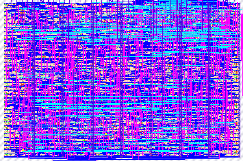
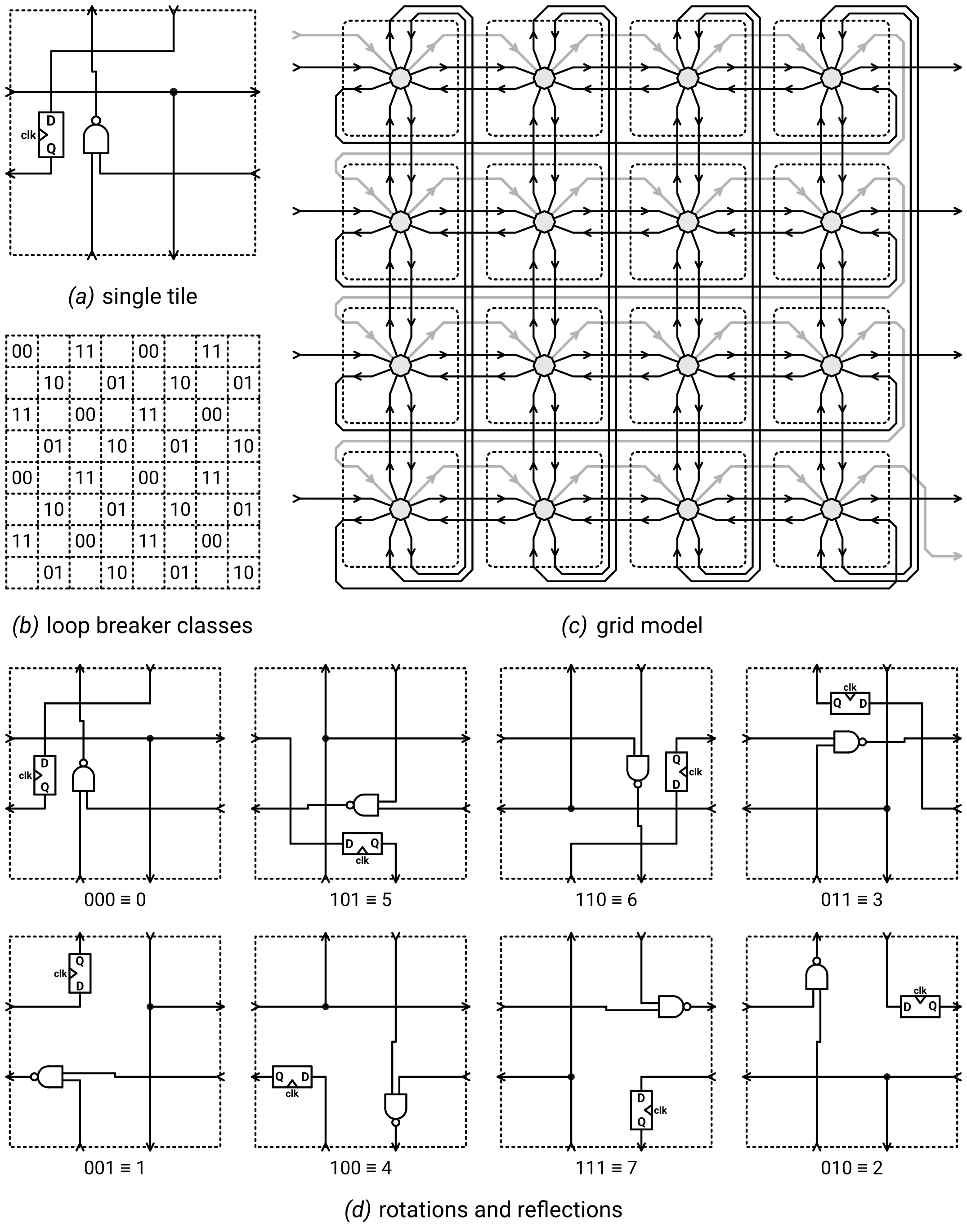
ROTFPGA v2 is a reconfigurable logic circuit built from identical copies of the tile in Figure (a) containing a NAND gate, a D flip-flop and a buffer, with each tile individually rotated or reflected as described by the FPGA configuration. It is a port of the original ROTFPGA from Caravel to TinyTapeout. Porting the design required a 50-fold decrease in chip area which was achieved using a combination of cutting corners, heavy optimization and a few design changes. In particular:
- The FPGA was reduced from 24×24 to 8×8 tiles. There are 8 inputs and 8 outputs instead of 12 each.
- To compensate for smaller size, tiles can also be mirrored in addition to rotation.
- Tiles (being the most repeated part of the design) were rewritten as hand-optimized gate-level Verilog.
- Each tile only contains 1 flip-flop (the one exposed to the user). Configuration is now stored in latches.
- Configuration and reset are performed using a routing-efficient scan chain, so the design is no longer routing constrained. This allows standard cells to be placed with >80% density.
- Openlane and its components are 2 years more mature, hardening the same HDL more efficiently.
Configuration
Each tile can be configured in 8 possible orientations. Bits 0, 1 and 2 correspond to a diagonal, horizontal and vertical flip respectively. Any rotation or reflection can be described as a combination as shown in Figure (d). (The bottom row looks somewhat different, but we just rearranged the wires so that the inputs and outputs line up with the unmirrored tiles.)
Tiles are arranged in an 8×8 grid:
- Top, bottom, left and right inputs and outputs are connected to the tile in the respective direction.
- Tiles mostly wrap around, e.g. the bottom output of a cell in the last line connects to the top input of the cell in the first line.
- As an exception to the wrapping rules, left inputs in the first column correspond to chip inputs and right outputs in the last column correspond to chip outputs.
- There is a scan chain meandering through all the tiles, visiting lines from top to bottom and within each line going from left to right.
Figure (c) shows a 4×4 model of the tile grid. When the scan enable input is 0, the FPGA operates normally and each tile sets its flip-flop to the input it receives from one of the neighboring tiles according to its current rotation/reflection (black arrows). When scan enable is 1, it sets the flip-flop to the value received through the scan chain instead (grey arrows). This allows us to set the initial state of each flip-flop and also to query their state later for debugging. With some extra machinery it also allows us to change the rotations/reflections.
When the 2-bit configuration input is is 01, each cell updates its vertical flip bit to the current value of its flip-flop. Similarly, for 10 it sets the horizontal flip and for 11 it sets the diagonal flip. When configuration is 00, all three flip bits are latched and the orientation doesn't change.
One can thus configure the FPGA by sending the sequence of all diagonal flip bits through the scan chain, then setting configuration to 11 and back to 00, then sending all horizontal flip bits, setting configuration to 10 and back to 00, and finally sending the vertical flip bits and setting configuration to 01 and back to 00.
Note that in order to save space the flip bits are stored in latches, not registers. Changing the configuration input from 00 to 11 or vice versa can cause a race condition where it is temporarily 01 or 10, overwriting the horizontal or vertical flip bits. Therefore one should configure the diagonal flips first.
Loop breaker
The user design may intentionally or inadvertantly contain combinational loops such as ring oscillators. To help debug such designs, the chip has a loop breaker mechanism using a loop breaker enable input as well as a 2-bit loop breaker class input.
Tiles are assigned to loop breaker classes according to Figure (b). The loop breaker latches a tile output if and only if the following conditions are all met:
- The loop breaker enable input is 1.
- The current tile has a non-empty class that is different from the loop breaker class input.
- The output doesn't come from the tile's flip-flop.
The loop breaker has the following properties:
- If loop breaker enable is 1 and loop breaker class is constant, there are no combinational loops running. If we also pause the clock, the circuit keeps a steady state.
- If loop breaker enable is 1 and we cycle loop breaker class through all possible values repeatedly while the clock is paused, everything will eventually propagate. If we also assume that the design has no race conditions, it will behave in the same way as if loop breaker enable was 0.
Reset
Setting the active-low reset input to 0 has the following effect:
- Override scan enable to 1, scan chain input to 0 and disengage the latches for vertical, horizontal and diagonal flips. When kept low for 64 clock cycles this will reset the state and configuration in every tile.
- Override loop breaker enable to 1 and loop breaker class to 00. This ensures that we play nice with other designs on TinyTapeout and keep a steady state while our design is not selected.
How to test
Follow the test suite in src/test.py.
IO
| # | Input | Output | Bidirectional |
|---|---|---|---|
| 0 | tile(0,0) left in | tile(7,0) right out | _scan enable_ input |
| 1 | tile(0,1) left in | tile(7,1) right out | _scan chain_ input |
| 2 | tile(0,2) left in | tile(7,2) right out | _configuration_ input bit 0 |
| 3 | tile(0,3) left in | tile(7,3) right out | _configuration_ input bit 1 |
| 4 | tile(0,4) left in | tile(7,4) right out | _loop breaker enable_ input |
| 5 | tile(0,5) left in | tile(7,5) right out | _loop breaker class_ input bit 0 |
| 6 | tile(0,6) left in | tile(7,6) right out | _loop breaker class_ input bit 1 |
| 7 | tile(0,7) left in | tile(7,7) right out | _scan chain_ output |
User feedback
- htfab👑: Follow the link for the test script. It covers reconfiguration, loading and dumping state, single stepping, free running and using the loop breaker. Link for more details