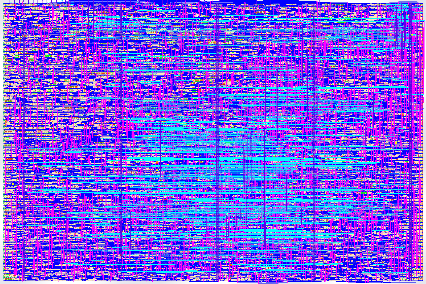
54 USB Device
54 : USB Device

- Author: Darryl Miles
- Description: USB FullSpeed/LowSpeed device (proof-of-concept)
- GitHub repository
- Open in 3D viewer
- Clock: 48000000 Hz
How it works
This text will be updated nearer the scheduled TT04 redistribution time (early 2024) along with the project github README.md and gh-pages documentation. Please regenerate your documentation.
This is a hardware implementation of a USB device end hardware interface, should be compliant with USB1.1 FS/LS (not HS).
It is designed to be driven and commanded by a CPU over a native bus (such as WishBone). Due to the limited IO ports with TinyTapeout there is a TT2WB WishBone driver that provides the ability to perform WishBone 32bit data-path transactions inside the module over the narrower TT IO ports. The hardware design is capable of being any kind of USB device, this includes (and it not limited to) CDC, HID, audio, storage as the CPU sets the identity of the device in software to the host.
While I intend to drive the TT IC with an FPGA development board myself, it should be possible for the RP2040 providing a 48MHz clock to this project to achieve some kind of hello world over USB. The controller clock uses the global CLK pin (this is expected to be 48MHz but may well work at a range of other clock rates), the PHY interface uses BIDI port 3 (this must be 48MHz to provide timing in both full-speed and low-speed modes).
You can fire WishBone commands at the TT2WB interface, this maps to most of the ports IN/OUT/BIDI. This is currently abstracted away (via API) for testbench purposes and it is intended this also be the case for the FPGA/RP2040 programming interfaces. At this time the best documentation around this is to look at the TT2WB.py and tt04_to_wishbone.v in the project.
The configuration options were reduced to squeeze something to demonstrate a working endpoint into a 2x2 tile space, this is possible because SpinalHDL is good a generating hardware designs based on complex parametrization that allow features to be turned on-off easily. The limited 2x2 tile space (ideally it wanted 2x4) has resulted in some limitations:
- the total number of endpoints is reduced from the full 16 down to 4 (numbered 0 to 3)
- the total buffer space available is reduced to just 52 bytes (this may be only enough space for a single active endpoint to operate, a standard serial CDC ideally need 3 endpoints working). The buffer space is provided by DFF registers and has a particular layout for control information and headers, this results in a total of 52 bytes only allowing a single endpoint to operate with a MaxPacketLen=8. If a 2x3 tile were possible 96-108 bytes of buffer would be possible which would allow 3 endpoints to operaten all at MPL=8 or a single endpoint at upto MPL=64 or some combination in between.
It is necessary to create a suitable USB cable to connect to the BIDI port0 and port1, this is expected to be the same cable and pinout scheme as the tt04-usbcbc project that is also present in TT04. This recommends a 68ohm series resistor for each of the Data+ and Data- lines, along with a pull-up resistor 1k5. The single pull-up resistor needs to be positioned appropriately for full-speed (on Data+) and low-speed (on Data-) modes.
How to test
This text will be updated nearer the scheduled TT04 redistribution time (early 2024) along with the project github README.md and gh-pages documentation. Please regenerate your documentation.
The original bus interface documentation can be found at https://spinalhdl.github.io/SpinalDoc-RTD/master/SpinalHDL/Libraries/Com/usb_device.html
The original source can be found at https://github.com/SpinalHDL/SpinalHDL/tree/dev/lib/src/main/scala/spinal/lib/com/usb/udc
This hardware was originally designed for FPGA so some modifications were made in the areas of:
- Improving USB specification (a couple of potential bugs/out-of-spec items)
- Use of combinational logic versions of CRC5/CRC16 function blocks.
- Fixing features that seemed 95 percent written and present in the code but obviously not working or tested (support dual full-speed and low-speed in same hardware stack)
- Running on ASIC (clocks/resets)
- Optimizing for ASIC (UsbTimer counter widths, DFF buffer reduction squeeze, endpoint reduction squeeze)
- Encapsulating WishBone bus inside a TinyTapeout User project.
- More items I've already forgotten on the way (but can document from code walk later)
The cocotb tests cover a significant number of the features and provide VCD output demonstrating almost everything possible with this hardware.
The Verilator/coverage showed the 2 main areas I do not exercise host suspend/resume and device resumeIt support. Plus a number of error scenarios and a few non-critial minor features of the hardware.
I hope by early 2024 to have available some FPGA and some RP2040 application code to assist demonstration.
External hardware
USB Connector, 2 x 68 ohm resistors, 1k5 ohm resistor
IO
| # | Input | Output | Bidirectional |
|---|---|---|---|
| 0 | tt2wb input bit0 | tt2wb output bit0 | USB D+ (bidi) |
| 1 | tt2wb input bit1 | tt2wb output bit1 | USB D- (bidi) |
| 2 | tt2wb input bit2 | tt2wb output bit2 | Interrupt (output only) |
| 3 | tt2wb input bit3 | tt2wb output bit3 | Phy Clock 48MHz (input only) |
| 4 | tt2wb input bit4 | tt2wb output bit4 | tt2wb control ACK (output only) |
| 5 | tt2wb input bit5 | tt2wb output bit5 | tt2wb control CMD bit0 (input only) |
| 6 | tt2wb input bit6 | tt2wb output bit6 | tt2wb control CMD bit1 (input only) |
| 7 | tt2wb input bit7 | tt2wb output bit7 | tt2wb control CMD bit2 (input only) |