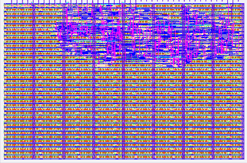
162 SAP-1 CPU
162 : SAP-1 CPU

- Author: Jayraj Desai
- Description: Implementaion of Simple As Possible (SAP-1) CPU based on the book Digital Computer Electronics by Albert Paul Malvino and Jerald A. Brown
- GitHub repository
- Open in 3D viewer
- Clock: 0 Hz
How it works
This project is an implementation of a CPU called SAP-1 as referred in the book 'Digital Computer Electronics' by Albert Paul Malvino and Jerald A. Brown. Book's PDF is available online, a simple internet search will point you to the PDF of the book. Difference in my implementation versus the one mentioned in the book is that they have used shared bus architecture, which was possible due to use of TTL tristate buffers but in CMOS implementation I am not aware of a simple way to infer a tristate buffer in verilog so made some changes to adapt their architecture. Another important thing to notice is that even though this project has full implementation of LDA, ADD, SUB and OUT instructions, I have not implemented interface to an external memory, instead I have hard coded a 16 x 8 bit memory in the memory_16x8_rom.v which kind of simulates memory. Hence this CPU can run only one code.
This Project needs two input only clk and rst_n. I plan to provide input clock by generating it outside using a 555 timer and using a simple switch to provide rst_n signal.
How to test
As mentioned in how it works this project needs two inputs clk and rst_n. Once these signals are applied after few clock pulses you should see output of a fixed
code at the output pins which can be viewed using set of 8 LEDs connected serially through resistors.
Expected output is binary 01 (This is output of first instruction that loads accumulator with value 01 which is stored at address 0x9 in memory) , 03
(This is output of second instruction which is add accumulator with value 02 which is stored at 0xA address in memory), 06
(This is output of third instruction which is add accumulator with value 03 which is stored at 0xB address in memory) and 02 (This is output of
third instruction which is subtract accumulator with value 04 which is stored at 0xC address in memory).
External hardware
Clock generator and a switch to provide reset signal
IO
| # | Input | Output | Bidirectional |
|---|---|---|---|
| 0 | clk = input clock | uo_out[0] | |
| 1 | rst_n = active low reset | uo_out[1] | |
| 2 | uo_out[2] | ||
| 3 | uo_out[3] | ||
| 4 | uo_out[4] | ||
| 5 | uo_out[5] | ||
| 6 | uo_out[6] | ||
| 7 | uo_out[7] |