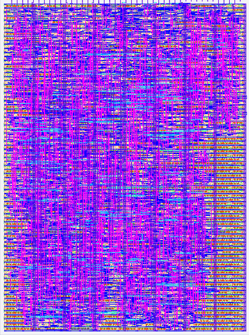
118 BFCPU
118 : BFCPU

- Author: Michael Yenik
- Description: Hardware BF CPU
- GitHub repository
- Open in 3D viewer
- Clock: 50000000 Hz
How it works
A hardware CPU for the brainfuck esolang, with some BFISA extensions!
The program and data memory don't remotely fit onto the given area, so they are handled externally using a custom asynchronous bus protocol. The bus can perform certain types of transactions (read data, write data, read char from I/O, write char to I/O, read next program word, read previous program word). These correspond to reading/writing data memory, reading program memory (the program counter is implicitly kept outside the BFCPU since it only requests next/prev instructions), and doing I/O (BF . and , instructions).
The bus is controlled by the BFCPU, with the BFCPU setting the bus type and ctrl pins, then setting the rdy output pin. When the bus device implementing the data/program/IO sees a rising edge on rdy, it looks at the type/ctrl pins to know what to do. In order to prevent bus conflicts, the BFCPU does not drive the bus unless the bus en pin is set by the bus device.
This allows the bus device to see the rising rdy edge, get ready to read whatever the BFCPU wants to put on the bus, set bus en, read it, and then unset bus en. If the BFCPU is trying to read something, then the bus device can simply drive the bus to the requested value.
Once the bus device has either read what the BFCPU has to say or driven the bus, it sets the ack input to the BFCPU to allow the BFCPU to continue the transaction. The BFCPU will accept the ack by setting rdy low, the device must continue to set ack until rdy goes low. In the case that the bus device is driving the bus to a requested value, it must continue to drive the bus until rdy goes low.
When a bus transaction is initiated, the type of transaction the CPU is trying to perform is put onto the bus type pins
- 000 - read data
- 001 - write data
- 010 - read char
- 011 - write char
- 100 - read next program byte
- 101 - read prev program byte
Since the data being read may be at an arbitrary 15 bit address, and we don't have enough pins to easily make address and data lines, the address and data are multiplexed onto the bus. When reading or writing from data memory, the address will be written onto the bus one byte at a time, then the data to be read/written will be placed onto the bus. In order to coordinate with the device on the bus about which phase of the transaction it's in, we use the two bus ctrl pins
- 00 - lower byte of address (for data read/write)
- 01 - upper byte of address (for data read/write)
- 11 - data phase (for data read/write, IO, and program read)
The BFCPU also supports a simple extension allowing from 2 up to 14 consecutive +, -, <, and > to be compressed into a-m, n-z, A-M, N-Z, respectively. So the following BF program '++++>>>>' can be compressed into 'cC'.
How to test
It needs a device paired with it that can read the bus signals and interpret the reads/writes correctly in order to operate. See the description above, as well as src/test.py in the github repo for an example. Hopefully there will also eventually be some RP2040 firmware in te repo to use with it!
External hardware
bus device (see above, probably RP2040 w/ fw)
IO
| # | Input | Output | Bidirectional |
|---|---|---|---|
| 0 | bus en | bus rdy | bus bit 0 |
| 1 | bus ack | bus ctrl bit 0 | bus bit 1 |
| 2 | bus ctrl bit 1 | bus bit 2 | |
| 3 | bus type bit 0 | bus bit 3 | |
| 4 | bus type bit 1 | bus bit 4 | |
| 5 | bus type bit 2 | bus bit 5 | |
| 6 | halted | bus bit 6 | |
| 7 | bus bit 7 |