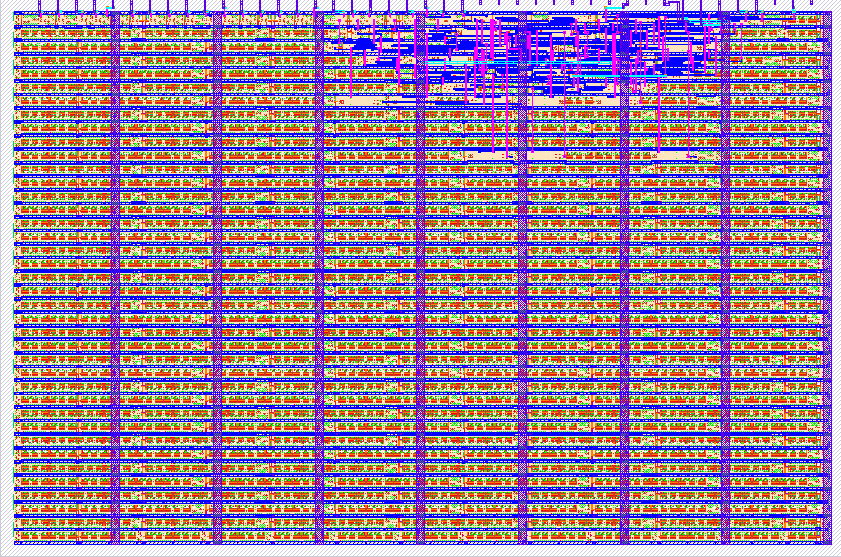
196 Test 4x4 memory
196 : Test 4x4 memory

- Author: Marchand Nicolas
- Description: A 4x4 memory adapted from :https://www.researchgate.net/figure/Structure-of-SRAM-Cell-The-design-of-SRAM-usually-involves-edge-triggered-flip-flops-The_fig3_324963843
- GitHub repository
- Open in 3D viewer
- View in Wokwi
- Clock: 1 Hz
How it works
it uses 16 flip flop logic to create the memory of 4 lines of 4bits
2 switches controle the lines, 4 switches sets the bits of a line, 2 switches setup the read and chip select (CS to be 1 to work), 4 outputs show the inverted value of the stored bit for the first line of 4 bits 4 outputs show the actual 4 bits of the selected line (updated by switching CS or RD)
truth table operation | CS | RD | Line1 | Line2 | In3 | In2 | In1 | In0 | Out3 | Out2 | Out1 | Out0 |
No operation | 0 | X | X | X | X | X | 0 | 0 | X | X | X | X |
Write operation | 1 | 0 | 0 | 0 | 1 | 0 | 0 | 0 | X | X | X | X | | 1 | 0 | 0 | 1 | 0 | 1 | 0 | 0 | X | X | X | X | | 1 | 0 | 1 | 0 | 0 | 0 | 1 | 0 | X | X | X | X | | 1 | 0 | 1 | 1 | 0 | 0 | 0 | 1 | X | X | X | X |
Read operation | 1 | 1 | 0 | 0 | X | X | X | X | 1 | 0 | 0 | 0 | | 1 | 1 | 0 | 1 | X | X | X | X | 0 | 1 | 0 | 0 | | 1 | 1 | 1 | 0 | X | X | X | X | 0 | 0 | 1 | 0 | | 1 | 1 | 1 | 1 | X | X | X | X | 0 | 0 | 0 | 1 |
How to test
Setting the input switch to on should store the data and turn the corresponding LED of the 7-segment ON or off regarding to the stored value.
External hardware
the switches and the 7-segment can be enough - either
IO
| # | Input | Output | Bidirectional |
|---|---|---|---|
| 0 | in 0 - updates the value of bit0 of the selected line with in4 and in5 | out 0 - segment a - value of bit0 of the selected line with in4 and in5 | |
| 1 | in 1 - updates the value of bit1 of the selected line with in4 and in5 | out 1 - segment b - value of bit1 of the selected line with in4 and in5 | |
| 2 | in 2 - updates the value of bit2 of the selected line with in4 and in5 | out 2 - segment c - value of bit2 of the selected line with in4 and in5 | |
| 3 | in 3 - updates the value of bit3 of the selected line with in4 and in5 | out 3 - segment d - value of bit3 of the selected line with in4 and in5 | |
| 4 | in 4 - selects the line with in5 | out 4 - segment e - control of bit0 of the first line (value Q-) | |
| 5 | in 5 - selects the line with in4 | out 5 - segment f - control of bit1 of the first line (value Q-) | |
| 6 | clk/step push-button to select write or read operation or can be automated on the clock | out 6 - segment g - control of bit2 of the first line (value Q-) | |
| 7 | in 7 - chip select, allways ON (1) to wrok | out 7 - dot - control of bit3 of the first line (value Q-) |