963 Lab and Lectures SoC
963 : Lab and Lectures SoC

- Author: Aloke Kumar Das
- Description: A tiny SoC comprising of a cpu, memory and SPI protocol
- GitHub repository
- Open in 3D viewer
- Clock: 50 Hz
How it works
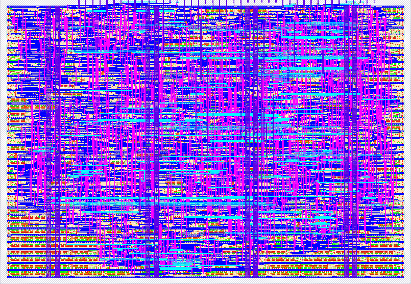
This project implements a tiny system on chip. It has a 16 bit microprocessor, a boot rom, a PWM, a timer and a spi protocol.
The boot rom has 32 words. After reset it runs a program to get input from outside and display to outside. The program has all the instructions that this processor supports. This tapeout is done to test the microprocessor on silicon. The SPI, PWM and timers are memory mapped. The processor writes the data to SPI, PWM and timers so that those IPs can be tested also.
The SPI protocol can be used for serial communication. The data can be loaded to and from cpu. This IP is mapped at 0020. If the cpu attempts to write to the address 0020 the data will be transmitted through the SPI protocol. It can accept data from outside of the SoC as specified in the spi protocol. The signals load and unload can be used to enable this IP.
The PWM resolution is 8. The duty cycle can be varied from 12.5 to 87.5 percent. It is memory mapped at the address 0040. It has a 3-bit register which can be written by the processor to set the duty cycle value. The timer is 8-bit without any pre-scalar. The timer is auto reload and can not be stopped. The output signals can be chosen from devide by 2/4/..../128. It is memory mapped at 0080. It has a 3-bit register which can be written by the processor to set the devisor value.
The microprocessor is a basic one. The data bus is 16-bits, address bus is 12-bits. Adderss and data busses are connected to internal boot rom, RAM and SPI. They cannot access outside memory. There is a parallel input port of 8-bits which is also input of the SoC. Similarly, there is a parallel output port of 8-bits that is also output of SoC. The Instructions that are supported are as follows: LDA - Load the content of a memory location to accumulatorAC ADD - Add the content of a memory location to AC AND - And the content of a memory location with AC STA - Store the content of AC to a memory location BUN - Branch unconditionally BSA - Branch to a memory location storing the return address ISZ - Increment the content of a memory location and check if zero, skip the next instructio Indirect addressing mode of all the above instruction are also supported
CLA - Clear the content of the AC CLE - Clear the overflow flag E CMA - Complement the content of the AC CME - Complement the overflow flag E CIR - Shift right the content of AC and E, circular CIL - Shift left the content of AC and E, circular INC - Increment the content of AC SPA - Skip next instruction if the content of AC is positive SNA - Skip next instruction if the content of AC is negative SZA - Skip next instruction if the content of AC is zero SZE - Skip next instruction if E is zero INP - Accept 8-bit input from input port if inp flag is high OUT - Send 8-bit output to output port and set the outp flag SKI - Skip next instruction if input flag is high SKO - Skip next instruction if output flag is high HLT - Halt the cpu
How to test
After power on the cpu starts running automatically. No extra effort is required. The boot rom has a program inbuit. It check for input. If input flag is high the 8-bit value is written to accomulator from ui_in pins. Immidiately the same value is output to uo_out pins so that it can be displayed on 7-segment. After that all the other instrustions are executed. Those tests the direct as well as indirect addressing modes. The program write addresses 0020, 0040 and 0080. This is the space for SPI, timer and PWM. The data comes out serially of uio_out[5] pin (mosi of spi), uio_out[4] and uio_out[3].
External hardware
Keypad, 7-segment or LCD or LED. Some kind of storage or data source. To be dicided later.
IO
| # | Input | Output | Bidirectional |
|---|---|---|---|
| 0 | keyboard 0 | display 0 | cpu keyboard in flag |
| 1 | keyboard 1 | display 1 | miso of spi |
| 2 | keyboard 2 | display 2 | ssn in of spi |
| 3 | keyboard 3 | display 3 | clock of spi (future use) |
| 4 | keyboard 4 | display 4 | ssn out of spi |
| 5 | keyboard 5 | display 5 | mosi of spi |
| 6 | keyboard 6 | display 6 | sclk of spi |
| 7 | keyboard 7 | display 7 | cpu display flag |