584 Tiny PLL
584 : Tiny PLL
- Author: LegumeEmittingDiode
- Description: 4-channel fractional-N frequency synthesizer
- GitHub repository
- Open in 3D viewer
- Clock: 10000000 Hz
How it works
Overview
This project showcases tiny_pll, a completely self-contained fractional-N
frequency synthesizer using less than 6% of the area of a 1x1 TinyTapeout tile.
The design goals of this project were as follows:
- The design should be as simple as possible to reduce the chance of failure.
- The design should be as small as possible so it can be incorporated into future Tiny Tapeout designs with minimal area overhead.
There are 4 tiny_pll instances in this project. Each instance multiplies the
frequency of a reference clock by a rational number A/B, where A and B can be
between 1 and 15. Such a block has two main use cases:
- Generating several internal clocks from a single off-chip oscillator (e.g., for a large digital design with multiple clock domains)
- Generating one or more internal clocks at a higher frequency than what can be provided to the tile through the mux and GPIO pins
tiny_pll is designed for a 10 MHz reference input, which implies an output
frequency between 67 kHz and 150 MHz. The 4 output clocks are connected to the
GPIO pins uo[3:0]. In reality, the maximum output frequency is limited by 4
factors:
- The speed of the Caravel I/O cells, which itself is a factor of the off-chip load capacitance
- The routing between the TT mux and the I/O cells
- The speed of the TT mux
- The routing between the project tile and the TT mux The minimum output frequency is limited to roughly 1 MHz due to the minimum speed of the VCO.
A 1-bit delta-sigma ADC is included to allow measurement of the analog control
voltage on uo[4].
This design is inherently mixed-signal due to the analog nature of the PLL.
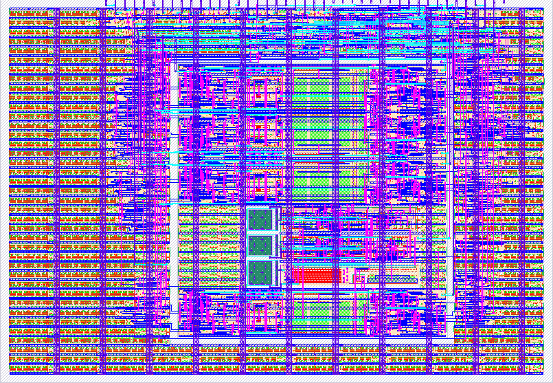
Consequently, the top-level layout is implemented as a custom analog/digital
section for the PLL and ADC, surrounded by RTL which implements the
control/status registers (CSRs) and various clock buffering and multiplexing
functions. Schematics were created using xschem and simulated with ngspice;
custom layout was done using klayout with the Efabless sky130 PDK; digital
synthesis and PnR was done using a custom OpenROAD flow; and magic and
netgen were used for LVS, DRC and parasitic extraction.
PLL
The top-level schematic of tiny_pll is shown below:
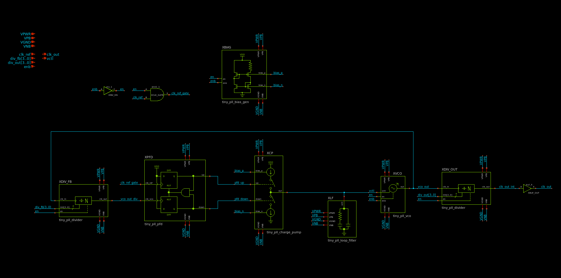
The PLL uses a standard fractional-N architecture, where an input and output
frequency divider are used to set the frequency multiplication with respect to
the reference clock input. The output frequency is A/B * f_ref, where A is
the division ratio of XDIV_FB, B is the division ratio of XDIV_OUT and
f_ref is the input clock frequency. Documentation for the PLL subcells is
included below.
Throughout the schematics, the pins VPB and VNB are included to connect the
bulk terminals of all PMOS and NMOS devices, respectively. This is done to
ensure the corresponding terminals of the standard cell instances at each level
of hierarchy are propagated to the top level and connected to VPWR and VGND.
Divider
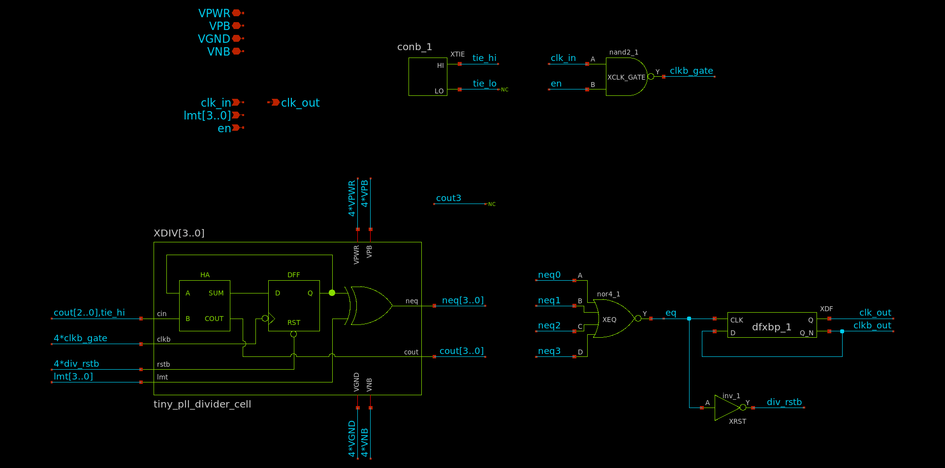
Frequency dividers are implemented using a 4-bit binary counter followed by 4
XOR gates to check for equality with a division ratio input lmt[3..0]. When
the counter output is equal to lmt, div_rstb is immediately asserted, which
resets the counter to 0 at the rising edge of clk_in. As a result, the maximum
division ratio from clk_in to eq is 15, when lmt == 4'b1111.
Since the counter is reset as soon as its output is equal to the division ratio,
a very short pulse is produced at the eq node, with a duration equal to the
propagation delay of the counter. This could potentially be a timing concern for
XDF, but since the counter delay is at least 3 gate delays, the flip-flop was
observed to operate as intended across process, voltage and temperature (PVT) in
simulation.
The D flip-flop (DFF) at the output is included to ensure an output duty cycle
close to 50%. As a result, the actual output frequency is f_ref / (2*lmt),
which implies a division ratio from clk_in to clk_out between 2 and 30.
The tie cell sky130_fd_sc_hd__conb_1 is used when gates must be connected to
VPWR or VGND to avoid potential ESD issues.
Phase-frequency detector (PFD)
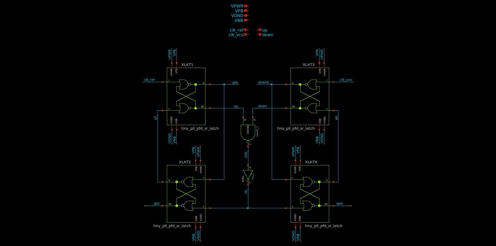
The PFD is composed of two DFFs, clocked by the divided VCO output and the
reference input, respectively. Since the input of both DFFs is tied to 1, each
DFF can be implemented using two S-R latches, each of which uses two nor2
gates. The full PFD thus uses 8 nor2 gates, one nand2 and one inv_1, which
is considerably smaller than using discrete DFF standard cells with the D inputs
tied to VPWR.
A NAND followed by an inverter is used instead of a single AND to slightly increase the minimum output pulse width and avoid charge pump glitches.
Charge pump
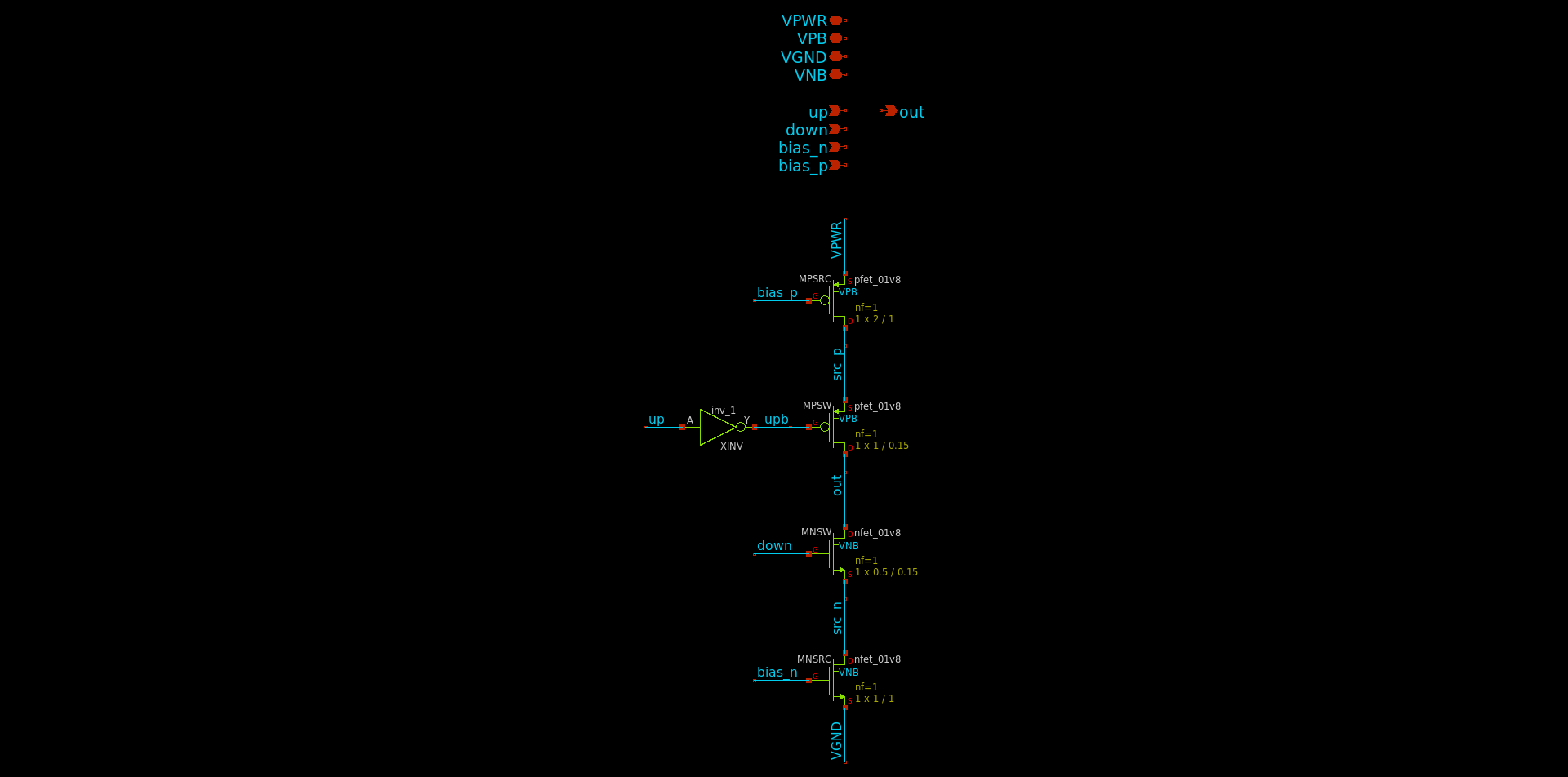
The charge pump uses two current sources (MNSRC and MPSRC), which can be
interchangeably switched to the output with the up and down inputs. The
charge pump current is nominally 1 uA and is set by the bias generator. The
switches use nearly minimum width to reduce area, and minimum length to reduce
capacitance. The PMOS switch uses 2x the W/L of the NMOS switch to ensure
roughly equal drain-source saturation voltages (VDSAT).
Loop filter
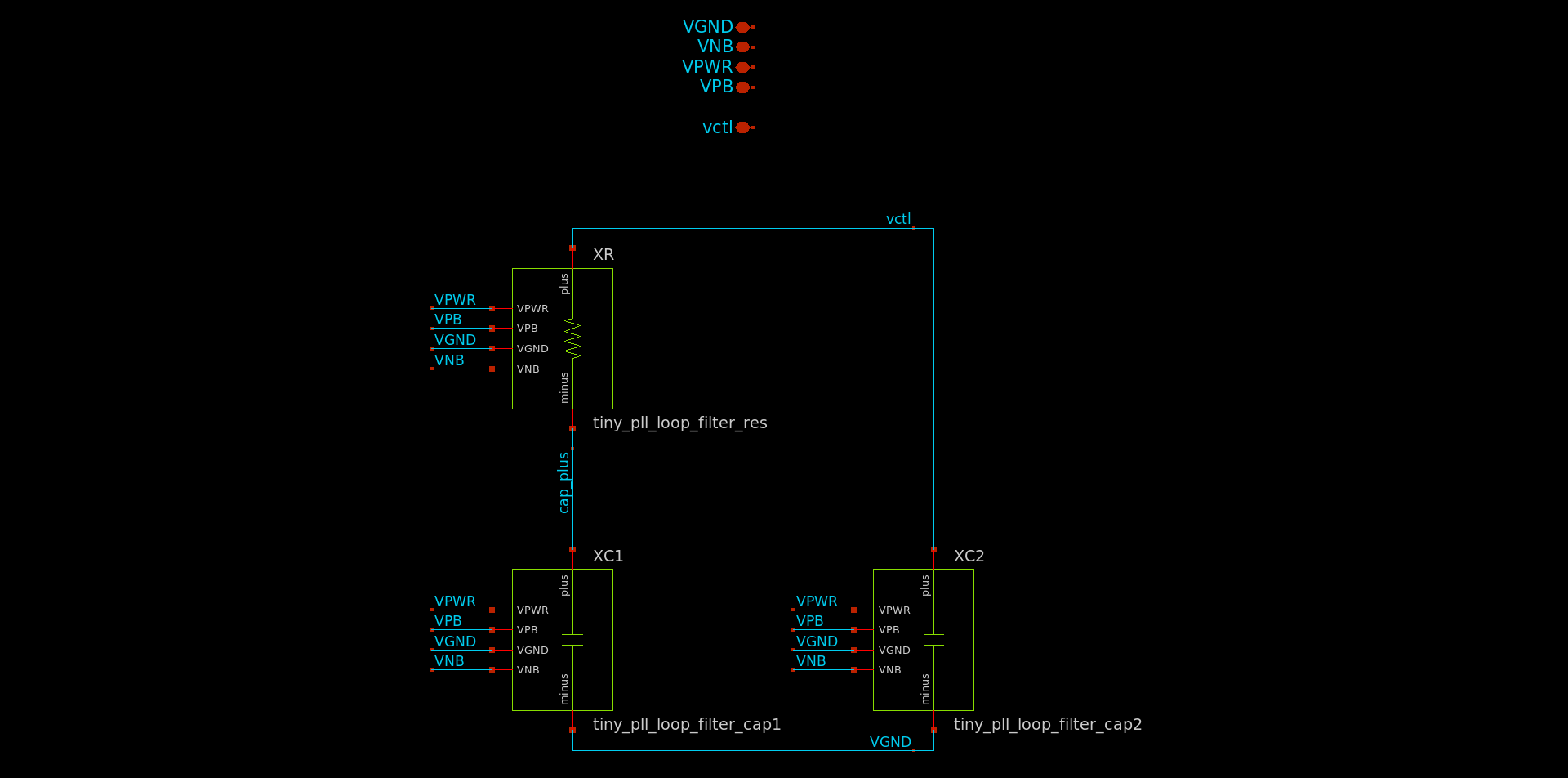
The loop filter is implemented using a series R/C combination to compensate the
loop transfer function such that a zero is placed below the crossover frequency
to ensure stability, and a pole is placed above the crossover frequency to
ensure fast settling time. A second capacitor XC2 is included to reduce ripple
in the control voltage, which in turn reduces phase noise at the PLL output.
Component values were selected using a linearized model developed using
schematic-only simulations of the VCO to determine the voltage-to-frequency
gain. The loop bandwidth was chosen to be on the order of 100 kHz, with a phase
margin of 65 degrees at an output frequency of 10 MHz. The resulting R/C values
are R = 100 kOhm and C1 = 1 pF.
In reality, the loop characteristics vary significantly across output frequency due to the nonlinear gain of the VCO, which was observed to have a nearly exponential voltage-to-frequency characteristic in simulation. This is likely due to the VCO current sources operating in the subthreshold region, where the ID/VGS characteristic is near-exponential.
The loop filter resistor is implemented using the urpm high-resistance poly
implant, which is roughly 2 kOhm/square. While e-test values are not provided
for this resistor in sky130, the value is not critical, and significant
variations (+/-50%) were observed to result in a stable loop in simulation.
The loop filter capacitors are implemented using NMOS devices with drain and source shorted to VGND. This is due to the significantly higher capacitance density of MOS devices relative to MIM capacitors (~8 vs ~2 fF/um^2). The MOS capacitance is highly nonlinear and increases at high control voltages due to the inversion charge, but again the capacitor value is not critical and this nonlinearity does not cause instability in the feedback loop.
The loop filter consumes nearly 50% of the area of the PLL. Various methods were explored to reduce loop filter area, including:
- MIM capacitors could be used and placed on top of the other circuit blocks to reduce area
- A capacitance multiplier could be used to allow a smaller intrinsic capacitance
The MIM capacitor method is possible, but there is some ambiguity in the
sky130 design rules as to whether a MIM capacitor can be placed over met1
and the base layers (see capm.10 in the sky130 periphery
rules.
Additionally, this could result in unwanted noise from the digital blocks
coupling into the capacitors, which could degrade phase noise performance.
Further, the capacitors would have to be divided up to lie between the power
rails on met4 which would increase their area.
A capacitance multiplier was implemented using a 100 fF capacitor with a 10:1 multiplication ratio, but the final layout was the same size as the MOS capacitor implementation and was thus exlcuded from the final design. The capacitance multiplier was additionally seen to have poor high-frequency response compared to a MOS or MIM capacitor, which resulted in unacceptably high control voltage ripple.
Voltage-controlled oscillator (VCO)
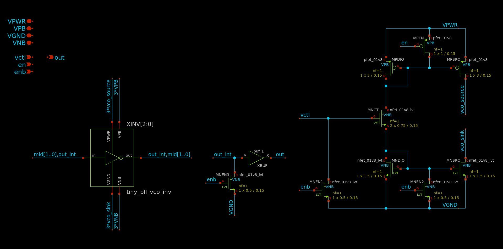
The VCO is a 3-stage current-starved ring oscillator using standard cell
inverters. The current sources are minimum-length to maximize W/L, which in turn
minimizes VDSAT, and minimize capacitance. The output resistance of these
current sources is irrelevant since it only matters that the oscillator current
is limited, and not the particular limit value. A triode device MNCTL is used
to control the source/sink current of the VCO. LVT NMOS devices are used to
ensure the operating control voltage is somewhere near half supply at an output
frequency of 10 MHz, which helps ensure the maximum output frequency can be met
across process variations. Four "keeper" devices (MNEN1, MNEN2, MNEN3 and
MPEN) are included to disable the circuit with zero static power consumption.
Bias generator
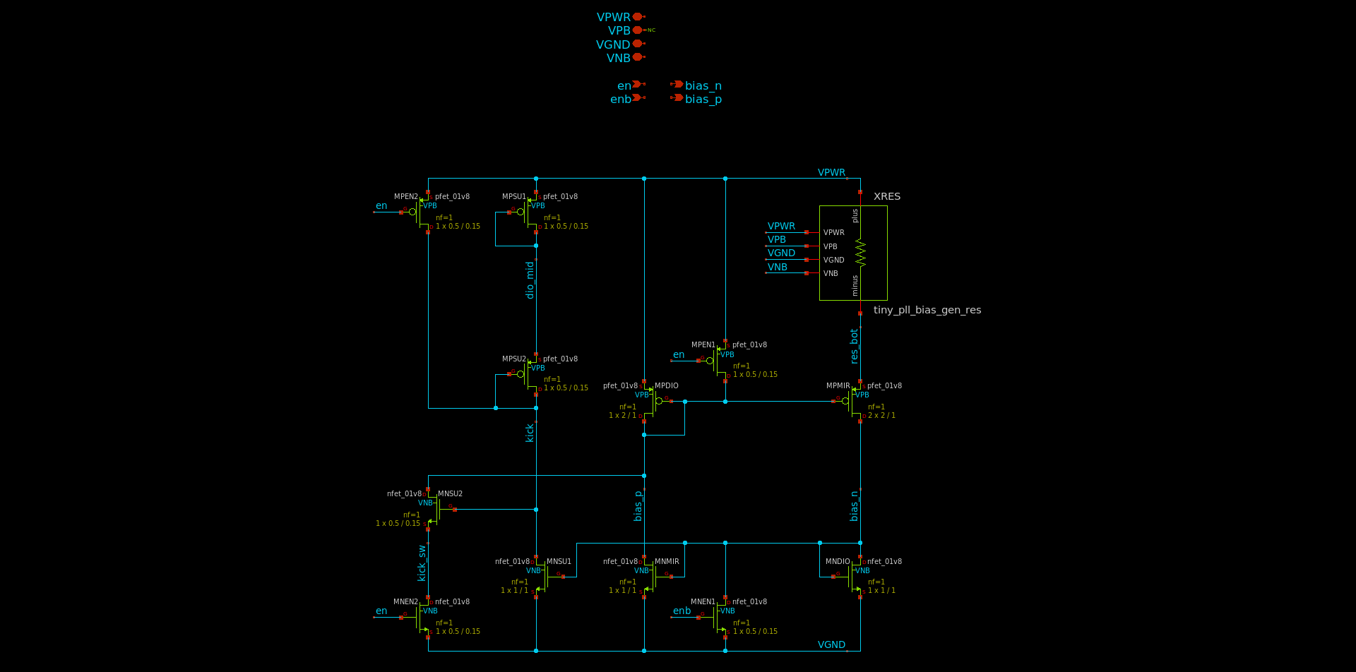
The bias generator is a self-biased current mirror, which provides a roughly
supply-independent current for the charge pump. The exact current is highly
dependent on the poly resistor XRES, but is designed to be nominally 1 uA at
25 degrees C. A startup circuit is included to ensure the bias generator does
not fall into an undesirable operating point where IOUT = 0. The diode devices
MPSU1 and MPSU2 charge the kick node to VPWR when the circuit is enabled,
which pulls bias_p low and establishes a current in the mirror devices. Once
the mirror is active, MNSU1 pulls kick low and disables the startup circuit.
Multiple "keeper" devices are included to disable the circuit with zero static
power consumption.
IO
| # | Input | Output | Bidirectional |
|---|---|---|---|
| 0 | csr_data_in[0]: Data input for PLL control registers | clk_out[0]: Channel 0 PLL clock output | clk_csr: Clock input for PLL control registers |
| 1 | csr_data_in[1]: Data input for PLL control registers | clk_out[1]: Channel 1 PLL clock output | |
| 2 | csr_data_in[2]: Data input for PLL control registers | clk_out[2]: Channel 2 PLL clock output | |
| 3 | csr_data_in[3]: Data input for PLL control registers | clk_out[3]: Channel 3 PLL clock output | |
| 4 | csr_addr_in[0]: Address input for PLL control registers | adc_out: Channel 0 control voltage ADC output | |
| 5 | csr_addr_in[1]: Address input for PLL control registers | ||
| 6 | csr_addr_in[2]: Address input for PLL control registers | ||
| 7 | csr_addr_in[3]: Address input for PLL control registers |