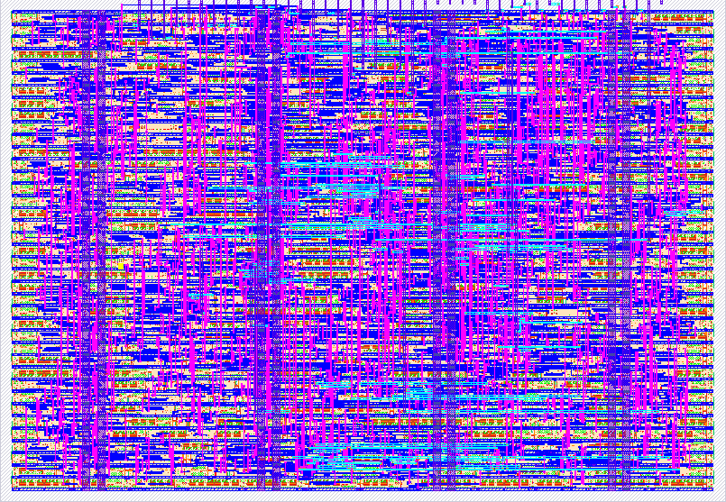
268 CEJMU Beers and Adders
268 : CEJMU Beers and Adders

- Author: Prof. Dr.-Ing. Matthias Jung, Philipp Wetzstein, Derek Christ, Jonathan Hager
- Description: Several projects to show in lectures. Includes a simple state-machine, a decoder and two 24 bit adders. Refer to documentation for details
- GitHub repository
- Open in 3D viewer
- Clock: 12000000 Hz
How it works
The goal of our design is to be able to show different RTL designs on a real chip in our lectures. Therefore, an internal multiplexer selects different projects. The multiplexer is controlled by uio_in[1:0]. The following designs can be selected:
- state machine that models a vending machine
- decoder to attach the vending machine to a coin acceptor
- 24 bit Ripple Carry Adder
- 24 bit Carry Lookahead Adder
How to test
- 00: A state machine, which models a vending machine. This state machine outputs 1, if 1.50€ have been fed into it. Inputs are taken from ui_in[1:0] with the following meaning: 00 = 0€ (nothing changes), 01 = 0.50€, 10 = 1€, 11 = undefined
- 01: A module that decodes pulses coming from a coin acceptor into coin ids. The number of pulses is equivalent with the decoded id. With a second instance of the vending machine automaton, this module makes it possible to physically insert coins into the machine.
- 10: Ripple Carry Adder with 24 bit input and 25 bit output
- 11: Carry Lookahead Adder with 24 bit input and 25 bit output
Since we only have 8 bit input and output, an internal logic is responsible for taking the inputs in 8 bit chunks and outputting the results in 8 bit chunks. This logic can be used as follows:
- Select the adder you want to use: uio_in[1:0] == 10 (RCA) or 11 (CLA)
- Reset the chip for at least one cycle
- ui_in[7:0] should now be assigned a[23:16]
- Wait for one cycle, repeat with a[15:8], a[7:0]
- Repeat with b[23:16], b[15:8], b[7:0]
- The inputs are now read into the design and will be send to the adders by asserting uio_in[2] to 1 (this is done to have a reference signal when measuring)
- If you are ready to read the outputs, set uio_in[3] to 1 and wait one cycle
- z[23:16] can now be read from uo_out
- Wait one cycle, z[15:8] can now be read
- Repeat for z[7:0]
Note that the overflows of both adders are always brought out to uio_out[7:6] to allow measurements. A reset upon changing the design is required to ensure valid results
External hardware
No external hardware is strictly required. Since the goal of both adders is to measure the difference in execution speed, an oscilloscope is helpful. The decoder for the coin acceptor was designed for the HX-916
IO
| # | Input | Output | Bidirectional |
|---|---|---|---|
| 0 | Multiplexed to all designs (refer to documentation for details) | Multiplexed from all designs (refer to documentation for details) | Select design (input) |
| 1 | ... | ... | Select design (input) |
| 2 | ... | ... | start_calc |
| 3 | ... | ... | output_result |
| 4 | ... | ... | unused |
| 5 | ... | ... | unused |
| 6 | ... | ... | overflow bit of RCA (output) |
| 7 | ... | ... | overflow bit of CLA (output) |