748 WokwiPWM
748 : WokwiPWM
- Author: Ken Pettit
- Description: A 4-channel PWM impelemented in PWM gates
- GitHub repository
- Open in 3D viewer
- View in Wokwi
- Clock: 10000 Hz
Wokwi 4-Channel PWM
As it says, this is a 4-channel PWM coded in Wokwi. Each channel has 3 8-bit values to control their frequency, duty cycle and relative (starting) phase to each other. Values are loaded by setting 8-bit data in on ui_in[7:0] and loading to the current address which auto-increments.
Block diagram
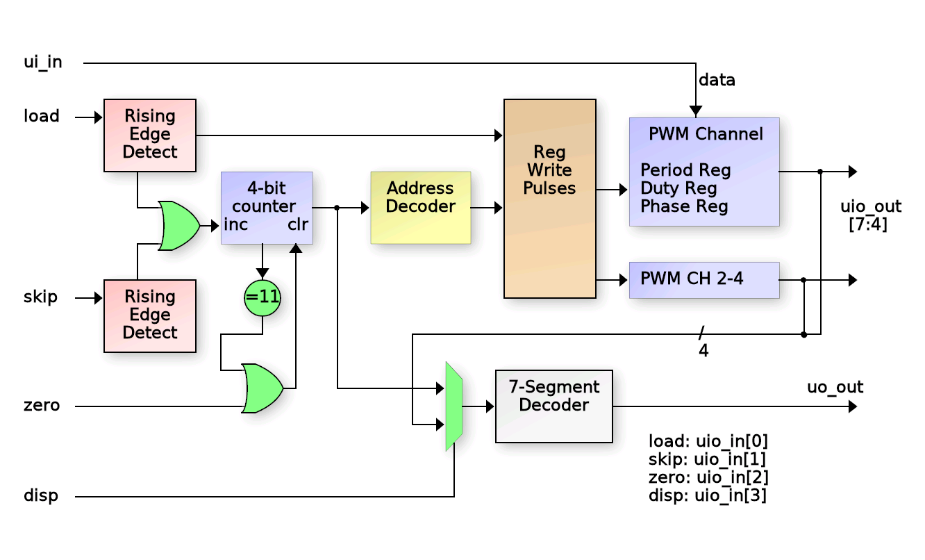
How it works
After reset, there is an 4-bit counter that is the address where the next 8-bit input data at in[7:0] will be loaded. The 'load' signal loads the 8-bit input to the register at that current counter address and then increments the counter.
The 'skip' input will skip an address without loading it. And the 'zero' input will reset the counter back to zero.
None of the 'load', 'skip', 'zero' or 'disp' inputs are debounced, but they are riging edge detected (at least the load and skip are).
The current count (register address) is displayed on the 7-segment display via a 4-to-7 decoder. Each of 4 PWM channels use two 8-bit control registers to set frequency and duty cycle. The first (lowest address) register controls the duty cycle and the second (highest address) controls the period of that channel. Only channels with non-zero period value will operate (the counter does not count when period_val is zero). For PWM channels 2-4, there is an additional 8-bit register (address 8-10) to control the starting phase of that channel relative to channel 1. This means that if channels 2-4 are to be used, channel 1 must also be used.
Program PWM channel control registers to create independent PWMs:
Address Meaning 0x0 PWM1 duty 0x1 PWM1 period 0x2 PWM2 duty 0x3 PWM2 period 0x4 PWM3 duty 0x5 PWM3 period 0x5 PWM4 duty 0x7 PWM4 period 0x8 PWM2 phase 0x9 PWM3 phase 0xa PWM4 phase 0xb Control BIT0: BIT1: BIT2: BIT3: Write '1' to clear and synchronize all PWM channels. Self clearing.
How to test
- Start the clock and reset the circuit.
- Set the DIP switches so only switch 7 is on (8'h40)
- Press 'load'. The display should now show '1'.
- Set the DIP switches so only switch 8 is on (8'h80).
- Press 'load'. The display should show '2' and the first LED should start blinking at about 50% rate.
- Continue programming values for the other 3 PWMs by setting DIP switch value and pressing 'load' even values (duty cycle) must be less that the associated odd address value (period).
- When the 7-segment display shows "8", this is the phase offset value for PWM channel 2 relative to channel 1. Loading a value here will force a known phase for channel 2 WHEN THE CHANNELS ARE SYNCHRONIZED.
- Load additional relative phase values for PWM channels 3 and 4 at the next two addresses (9 and A).
- To synchronize the PWM channels, write a value of 4 to address B.
External hardware
LEDs should be connected to the PWM channel outputs. The 7-Segement display shows the current register address to be written.
IO
| # | Input | Output | Bidirectional |
|---|---|---|---|
| 0 | D0 | seg_a | load |
| 1 | D1 | seg_b | skip |
| 2 | D2 | seg_c | zero |
| 3 | D3 | seg_d | disp |
| 4 | D4 | seg_e | pwm_0 |
| 5 | D5 | seg_f | pwm_1 |
| 6 | D6 | seg_g | pwm_2 |
| 7 | D7 | seg_dp | pwm_3 |