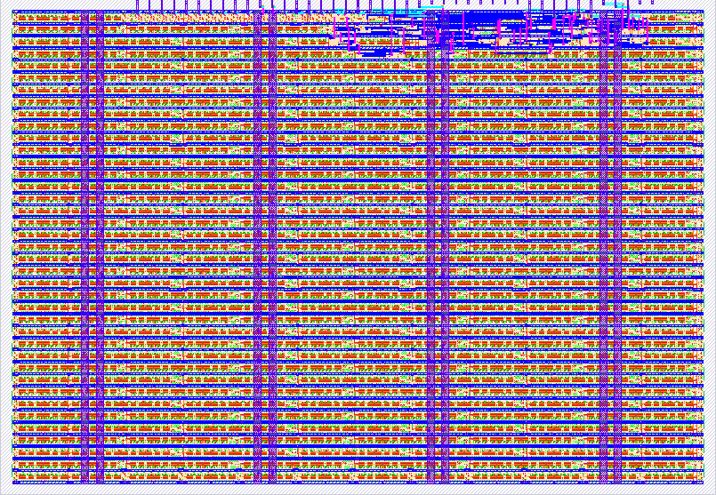
418 DETDFF (Tiny Tapeout)
418 : DETDFF (Tiny Tapeout)

- Author: Patrick D. Lloyd
- Description: 4x Dual-Edge-Triggered D-Flip Flops for Tiny Tapeout
- GitHub repository
- Open in 3D viewer
- View in Wokwi
- Clock: 0 Hz
How it works
This is a collection of four D-type flip-flops that each load & store the input, D, to output, Q, on either the rising or falling clock edge. There are also asynchronous RESET inputs.
Although there are inputs on the DETDFFs called "CLK", the application this circuit was designed for doesn't utilize a traditional periodic input waveform. The Tampercut project aims to use this circuit as a way to detect if the physical enclosure of a computer server is jostled, tilted, or tampered with. The idea is to connect various binary sensors to the CLK inputs, and set D to VCC (logic high). Then, when a sensor triggers (either active-high or active-low), even briefly, the logic-high value will be latched to the output, Q. This persistent state will remain on the output until the DETDFF is explicitly reset, either through the RST_N button, or by driving D low and manually clocking the sensor trigger. QN doesn't really serve much purpose except providing a complementary output on the 7-segment display.
How to test
This circuit does not make any use of the provided clock input, only the piano input switches and the RST_N button. The design won't build properly with a floating clock so there is a bogus inverter in the design not connected to anything to get the Github Actions to pass. The outputs, Q, of the DETDFFs and their complements, QN, are shown on the 7-segment display:
DETDFF0 (D0 / IN0, CLK0 / IN1) -> Q0  (Top Segment          /  A)
                               -> QN0 (Bottom Segment       /  D)

DETDFF1 (D1 / IN2, CLK1 / IN3) -> Q1  (Top Left Segment     /  F)
                               -> QN1 (Top Right Segment    /  B)

DETDFF2 (D2 / IN4, CLK2 / IN5) -> Q2  (Bottom Left Segment  /  E)
                               -> QN2 (Bottom Right Segment /  C)

DETDFF3 (D3 / IN6, CLK3 / IN7) -> Q3  (Dot LED              / DP)
                               -> QN3 (Middle Segment       /  G)
- Inital conditions: All D pins should be set to ON (connecting the inputs to VCC). CLK pins can be set to ON (VCC) or unset to OFF (GND) arbitrarily. Press RST_N to zero out the flip-flop outputs. The display should show F (for Fun).
- Operation: Any toggleing of a CLK will cause the corresponding segment and its complement to toggle and stay in that toggled state until either a reset, or a logic-low on the D input is clocked in.
External hardware
No external hardware is required for testing, but take a look at Tampercut for more info on this project's application.
IO
| # | Input | Output | Bidirectional |
|---|---|---|---|
| 0 | D0 | Q0 | |
| 1 | CLK0 | QN0 | |
| 2 | D1 | Q1 | |
| 3 | CLK1 | QN1 | |
| 4 | D2 | Q2 | |
| 5 | CLK2 | QN2 | |
| 6 | D3 | Q3 | |
| 7 | CLK3 | QN3 |