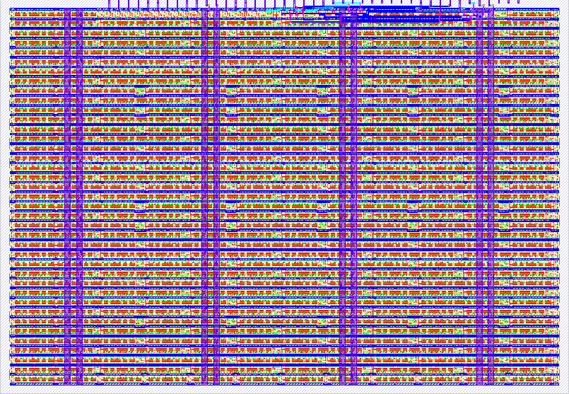
The circuit uses logic gates (AND, NAND, and OR) to process two binary inputs. The inputs are set using the DIP switch, and the outputs are displayed through a 7-segment display.
A clock (triggered by the Step button) sends pulses to the system. Each press advances the logic state. A Reset button clears the circuit to its initial state.
The Input block receives 8 input bits (from the DIP switch). The Output block shows the results of logic operations on the display. The 7-segment display represents the logic result in visual numeric form.
Press RESET to clear the circuit.
Set the DIP switch inputs (e.g., IN0 and IN1 for a and b).
Press STEP to clock the circuit and update the display.
Observe the 7-segment output or output pins.
Compare the results with the expected logic table below:
| Input A | Input B | Output AND | Output NAND | Output OR |
|---|---|---|---|---|
| 0 | 0 | 0 | 1 | 0 |
| 0 | 1 | 0 | 1 | 1 |
| 1 | 0 | 0 | 1 | 1 |
| 1 | 1 | 1 | 0 | 1 |
Optionally, connect a clock source (e.g., 10 kHz) to the CLK pin to automate stepping. You should see the outputs (and segments of the display) flashing at different rates depending on the logic combination.
List external hardware used in your project (e.g. PMOD, LED display, etc), if any
| # | Input | Output | Bidirectional |
|---|---|---|---|
| 0 | Clock (Step button) | Output 0 (to 7-segment display segment a) | Not connected |
| 1 | Reset (active LOW) | Output 1 (to 7-segment display segment b) | Not connected |
| 2 | IN0 from DIP switch | Output 2 (to 7-segment display segment c) | Not connected |
| 3 | IN1 from DIP switch | Output 3 (to 7-segment display segment d) | Not connected |
| 4 | IN2 from DIP switch | Output 4 (to 7-segment display segment e) | Not connected |
| 5 | IN3 from DIP switch | Output 5 (to 7-segment display segment f) | Not connected |
| 6 | IN4 from DIP switch | Output 6 (to 7-segment display segment g) | Not connected |
| 7 | IN5–IN7 from DIP switch (unused in logic) | Output 7 (extra/unused output) | Not connected |