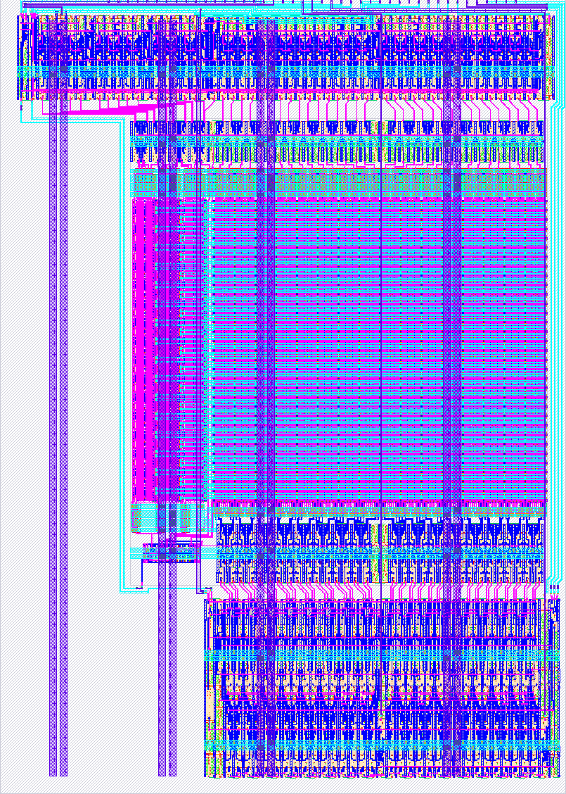
576 TTSKY25B Register File Validation
576 : TTSKY25B Register File Validation
- Author: Sylvain Munaut
- Description: Validation design for register file macro
- GitHub repository
- Open in 3D viewer
- Clock: 0 Hz
The register file
The register file macro being tested is an optimized SRAM macro organized as 32 words of 32 bits and offers three access ports : One write port and two read ports.
It's been designed for TinyTapeout especially. It's compact enough ( ~ 88% of the area of a single tile ) and doesn't use any DRC waiver/special rules.
The interface looks like this :
module rf_top (
    input  wire [31:0] w_data,
    input  wire  [4:0] w_addr,
    input  wire        w_ena,
    input  wire  [4:0] ra_addr,
    input  wire  [4:0] rb_addr,
    output reg  [31:0] ra_data,
    output reg  [31:0] rb_data,
    input  wire        clk
);
The internal working of the macro are out-of-scope for this document.
The validation design
This particular documentation focuses on this specific design which is meant to validate the register file macro, both from a functionality stand point but also its timings.
This is the high-level overview of the design :

The main blocks are :
- A generator block that controls all the inputs to the register file, feeding all the read/write addresses and write data.
- The register file itself.
- A capture and compare block that captures all the outputs of the register file and can compare them either to a known value or against a LFSR sequence.
Each of those blocks is clocked independently which should allow to test the various timings (setup/hold/clock-to-out/retain) by phase shifting them against each other.
In addition, there is a small "feedback" block that can select 4 timing critical signals and feed them back to an output through a common path. This should allow to calibrate out any skew in the input path of those signals to make more precise timing measurements.

Generator
The high level overview of the generator block is show below :

It's composed of 6 blocks, each with an internal shift register chain. They are chained together in a single chain, as shown, new data being fed to the MSB first.
There are two types of block :
- One "common" type of variable length to generate write data and read/write addresses.
- One special type to generate the write enable signal specifically.
The common block internally looks like this :

It first starts with two independent bit elements in the chain, and then follows a multi bit element that can be either 5 or 16 bits long.
When the global_mode signal is low, the whole block acts as a shift
register which allows to load arbitrary values anywhere in the chain.
Note that when the signal is low, the output of the block is also masked
and forced to zero. This avoid having the register file see randomly
changing inputs while loading new values.
When the global_mode signal is high then the two first bits don't
change any more and they instead define two control signals local to
this specific block : local_mode and local_ena.
The first one local_mode defines how the block acts when clocked.
Either the value stays the same across clock cycle, remaining whatever
was loaded serially. Or the values goes through a LFSR. The polynomial
is either 0xD008 or 0x14 depending on the length (both being maximum
length). Note that like any LFSR if you pre-loaded zero, the value will
remain zero. And that if you pre-loaded any other value, then zero will
never be generated.
The second control bit local_ena can force this group to be unmasked
even if the global masking signal global_ena is not active. This can
be used to independently test the setup/hold times requirements of the
data/addresses, forcing all the groups to be active except the one
under test, and then using global_ena to unmask the group under test
slightly before/after clock edge.
The WE signal is generate a bit differently :

There is only one control bit local_ena that operates the same way
as for the common block. But the actual value is fed through a dedicated
input signal we_in.
Capture
The capture block is very simple. It's composed of two blocks chained together, each handling 16 bits from read port A and 16 bits from read port B.

The actual shift chain is actually composed of 34 bits, the two lower bits are control bits and then 32 bits of data, with the two read port interlaced.
There is a cap_sel signal that controls if the capture block is
operating in "shift" mode, where the data that was previously captured
can be shifted out, but also new data can be shifted in from the outside.
This way you can both read what was captured, but also load controlled
data into the chain.
If the shift mode is not enabled, when cap_sel is low, then the two
control bits are fixed and don't change on the clock edge. The data
bits are simply captured directly from the register file data outputs.
The output of the capture block is selected by one of those control bits. It only outputs either the values capture from read port A or of read port B. This is simply because the following compare block was a bit too large and I couldn't fit two of them, so automatic comparison tests are limited to a single port at a time.
Compare
The compare block is depicted below.

Its purpose is to be able to directly compare captured data with expected value. Those can either be a fixed value, or a LFSR sequence, the same as generated by the generate block.
There is a group local signal group_mode that comes from the capture
block and selects the operation mode, either fixed value or LFSR.
The two other control signals rst and exec are global. The former
just resets the latching error signal to zero. The second one select
if we're pre-loading the LFSR or comparison value, for initialization
purposes, or if we're executing the comparison.
Typically, you'd preload some value in the capture stage using
shift register, then clock once with exec set to zero to configure
the compare stage and then automated comparison can begin.
There are some subtleties to the exact sequence to follow to properly synchronize generate and compare stage to properly automate long tests, but it is possible (tested in a verilog test bench).
How to test
No test procedure has been written yet. It's probable that at some point some custom test script for the demo board will be written to run functional tests but this is not done yet.
External hardware
The design itself doesn't use any external hardware and nothing should be connected to the PMODs of the demo board.
Basic functional testing is possible with the default demo board, controlling signals through the pico microcontroller.
However to do any advanced timing testing, measuring setup/hold times and such, very fine timing control will be needed. A scope will be needed to measure the skew between the critical control signals using the "feedback" mechanism and then some FPGA hardware will need to be used to have precise timing control of the signals sent to the design to make measurements.
The exact testing platform is still TBD.
IO
| # | Input | Output | Bidirectional |
|---|---|---|---|
| 0 | cmp_rst | cap_dat_out | |
| 1 | cmp_exec | k_zero | clk_cap |
| 2 | cap_sel | cmp_err_msb | |
| 3 | gen_dat_in | cmp_err_lsb | clk_gen |
| 4 | we_in | k_zero | |
| 5 | cap_dat_in | k_zero | clk_rf |
| 6 | gen_glb_ena | fb_out | fb_sel[0] |
| 7 | gen_glb_mode | k_zero | fb_sel[1] |