580 Open FGPA 2x2 design
580 : Open FGPA 2x2 design
- Author: Zhenyuan Liu
- Description: A small 2x2 CLB fpga
- GitHub repository
- Open in 3D viewer
- Clock: 1000000 Hz
How it works
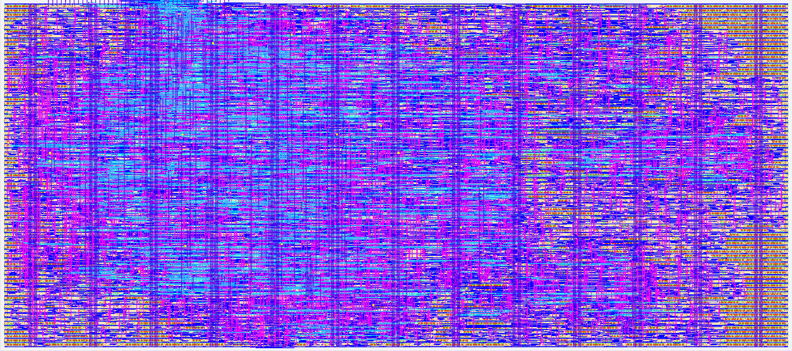
This project is built on a 2×2 OpenFPGA fabric that contains 4 configurable logic blocks (CLBs), 8 I/O blocks, 9 switch boxes (SBs), and 12 connection boxes (CBs). The CLBs implement user-defined logic, the I/O blocks provide external interfacing, and the SBs and CBs form the programmable routing network that connects logic to I/O. A Verilog design is compiled into a bitstream that configures these resources, allowing the fabric to function as the intended digital circuit.
How to test
To test the project, load the generated bitstream onto the 2×2 OpenFPGA fabric and drive input signals through the I/O blocks. The outputs can be observed on the corresponding I/O pins and verified against expected results, either in simulation or with external measurement equipment such as a logic analyzer.
External hardware
No dedicated peripherals are required. The design uses the FPGA’s I/O blocks directly for input and output, with optional use of standard lab equipment such as signal generators for inputs or logic analyzers for outputs during hardware evaluation.
IO
| # | Input | Output | Bidirectional |
|---|---|---|---|
| 0 | gfpga_pad_GPIO_PAD_fm[35] | gfpga_pad_GPIO_PAD_fm[48] | gfpga_pad_GPIO_PAD_fm[47] |
| 1 | gfpga_pad_GPIO_PAD_fm[41] | gfpga_pad_GPIO_PAD_fm[26] | gfpga_pad_GPIO_PAD_fm[31] |
| 2 | gfpga_pad_GPIO_PAD_fm[34] | ccff_tail_fm | ccff_head_fm |
| 3 | gfpga_pad_GPIO_PAD_fm[42] | gfpga_pad_GPIO_PAD_fm[11] | prog_clk_fm |
| 4 | gfpga_pad_GPIO_PAD_fm[28] | gfpga_pad_GPIO_PAD_fm[22] | set_fm |
| 5 | gfpga_pad_GPIO_PAD_fm[55] | gfpga_pad_GPIO_PAD_fm[36] | gfpga_pad_GPIO_PAD_fm[0] |
| 6 | gfpga_pad_GPIO_PAD_fm[33] | gfpga_pad_GPIO_PAD_fm[45] | gfpga_pad_GPIO_PAD_fm[30] |
| 7 | gfpga_pad_GPIO_PAD_fm[40] | gfpga_pad_GPIO_PAD_fm[63] | gfpga_pad_GPIO_PAD_fm[50] |