490 mini mosbius
490 : mini mosbius
- Author: andrew kang
- Description: a mosbius style chip in a 3x2 tt slot
- GitHub repository
- Open in 3D viewer
- Clock: 0 Hz
How it works
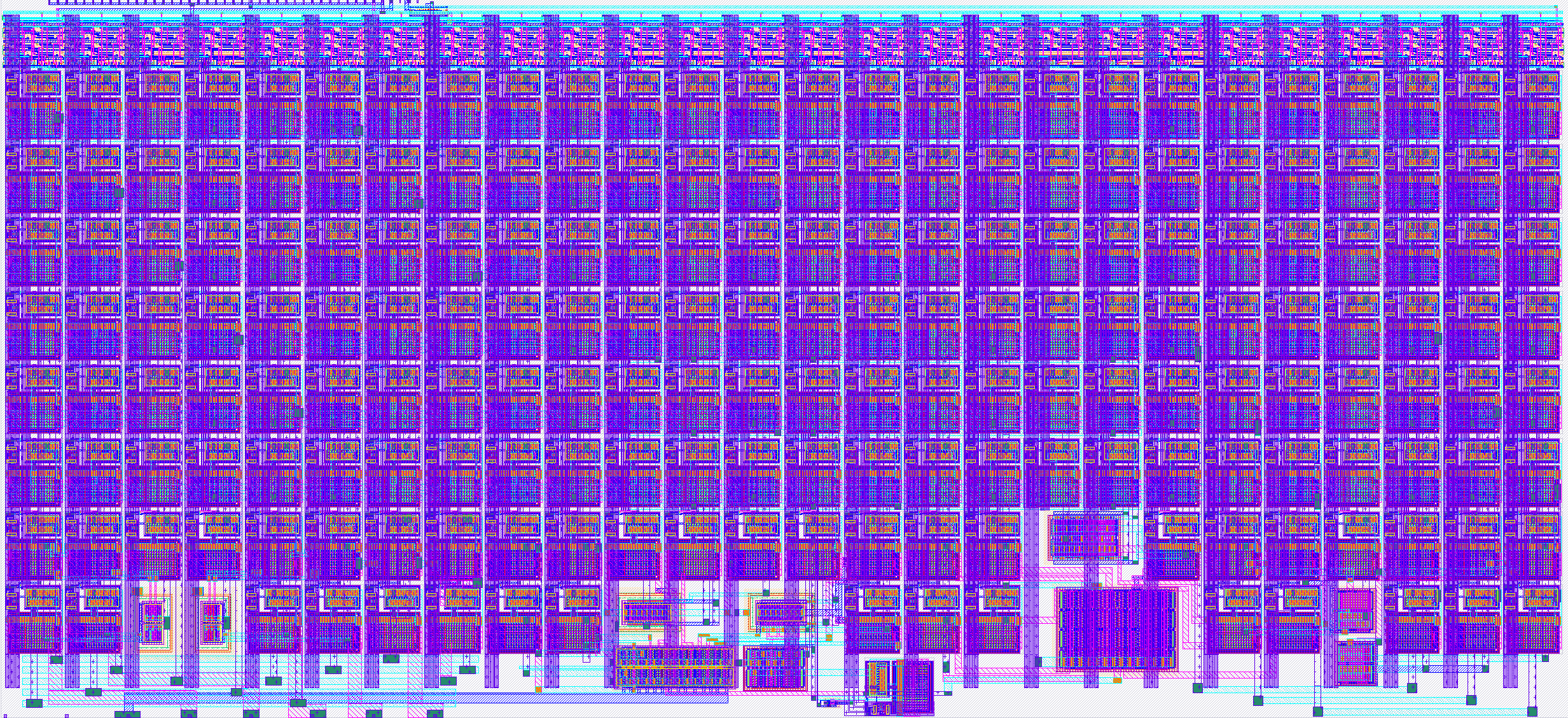
A mini MOSbius in a 3x2 tiny tapeout slot.
Contains the following blocks (x2) NMOS, programmable width (x2) PMOS, programmable width (x1) N-type differential pair, programmable tail current (x1) P-type differential pair, programmable tail current (x1) N-type 5T-OTA, programmable tail current (x2) N-type current sources (referenced to input bias current), programmable current (x2) P-type current sources (referenced to input bias current), programmable current
6 busses, 5 of which can connect to external package pins, are available to interconnect the blocks.
Each of the 6 busses contains A and B sides, which can be electrically shorted (single A/B bus) or isolated (separate A and B busses).
Contains 196 transmission gates to interconnect the blocks. Programming is done by a shift register.
Generating the programming file is WIP.
How to test
Provide a 100uA bias current into the "ibias" pin.
Toggle "rst_n" low then release to high to set shift register back to zero.
Hold "enable" low until shift register programming is done. This gates the shift register output to prevent random states until programming is done.
Clock in 196 bits to the shift register using "clk" and "dat_in". Sampled on posedge of "clk".
When programming is completed, assert "enable" high to set transmission gates.
Analog I/O is on "bus5" through "bus1" pins.
"data_out" is typically unused, except for debugging.
External hardware
Raspberry Pi or digital pattern generator to program the device.
Application dependent equipment to interface with the "bus5"-"bus1" pins.
IO
| # | Input | Output | Bidirectional |
|---|---|---|---|
| 0 | dat_in | dat_out | |
| 1 | enable | ||
| 2 | rst_n | ||
| 3 | |||
| 4 | |||
| 5 | |||
| 6 | |||
| 7 |
Analog pins
ua | PCB Pin | Internal index | Description |
|---|---|---|---|
| 0 | A5 | 5 | bus1 |
| 1 | A0 | 0 | bus2 |
| 2 | A4 | 4 | bus3 |
| 3 | A1 | 1 | bus4 |
| 4 | A3 | 3 | bus5 |
| 5 | A2 | 2 | ibias |