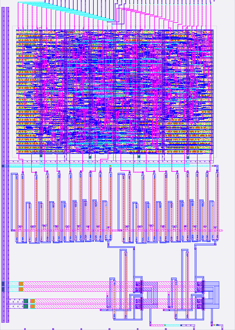
780 Simple audio player
780 : Simple audio player

- Author: Michael Bikovitsky
- Description: Plays audio from an SPI flash chip
- GitHub repository
- Open in 3D viewer
- Clock: 1536000 Hz
How it works
Plays raw unsigned 8-bit PCM samples read from an attached SPI flash
through DACs connected to analog pins ua[0] and ua[1].
How to test
Production mode
The audio data should be stored on the flash chip as a sequence of raw unsigned 8-bit PCM samples, left channel, then right channel. A stereo file can be converted into this format using FFmpeg:
ffmpeg -i /path/to/input/file -c:a pcm_u8 -f u8 /path/to/output/file
After flashing this to the chip, do the following:
- Set
uio[7]high. - Provide a clock signal to the chip according to the following formula:
clock_hz = sample_rate_hz * 16 * 2.- For example, if the audio is at 44.1 kHz, supply a clock of 1411.2 kHz.
- For 48 kHz, supply a clock of 1536 kHz.
- Pull the
rst_nsignal low, then pull it high. - Set
ui[0]high to start playback. - Set
ui[0]low to pause. Setting it high it again will resume from the same position.
In this mode, one of the two audio channels is also mirrored
on the uo pins: the left channel if uio[6] is high, and the right
channel if it is low. Whenever a new sample is sent to the DAC,
it is also mirrored to these pins.
While the player is playing audio, uio[4] will be high.
Note that in the QSPI Pmod
uio[4] is connected to IO2, which is the WP# pin on the flash.
Since we're only ever reading from the flash, there shouldn't be a
problem reusing this pin for another indication.
This wasn't tested pre-silicon, so YMMV.
Another note for the QSPI Pmod: uio[7:6] are the CS# pins for
the SRAM chips. They have a pull-up resistor though, so in the default
configuration everything should work fine. Again, YMMV.
Test mode
When uio[7] is low, the design is in test mode.
The 8-bit value on the ui pins is passed directly to the DAC
(ua[1] if uio[6] is high, ua[0] if it is low). This can be used
to test the DACs themselves.
In this mode, the SPI controller is also directly exposed:
ui[7:0]- Addressuio[4]- Data validuio[5]- Read enableuo[7:0]- Data output
When the "read enable" pin is asserted (high), the controller will start reading from the flash chip starting at the given address. When a byte has been read, the "data valid" signal will be asserted for a single clock cycle, and the data presented on the "data output" pins.
The controller will continue reading bytes from sequential addresses until the "read enable" bit is deasserted.
(The SPI controller can read from any 24-bit address on the flash, but we don't have enough input pins to expose the whole address range for debugging.)
If you're using the QSPI Pmod, note that uio[4] and uio[5] are
connected to IO2 and IO3. IO2 is the WP# pin, so it should be fine to
toggle it since we're only ever reading from the flash. That's why it's
the "data valid" output in this mode. uio[5] is IO3, which is HOLD#/RESET#,
so using it for "read enable" should also be fine.
This wasn't tested pre-silicon, so YMMV.
Also note that to use the Pmod and the debug mode, the CS# traces
for the SRAM chips will have to be cut. Otherwise, pulling uio[7:6]
low will activate these chips.
External hardware
SPI flash connected as follows:
uio[0]- CS#uio[1]- IO0uio[2]- IO1uio[3]- SCLKuio[4]- IO2uio[5]- IO3
This pinout should be compatible with the QSPI Pmod. Read the "How to test" section above for more notes about this Pmod.
The flash must be configured to accept 24-bit addresses with
the READ command (0x03).
Audio amplifiers connected to ua[0] and ua[1]. Exact specs TBD.
IO
| # | Input | Output | Bidirectional |
|---|---|---|---|
| 0 | Play/pause (DAC passthrough / SPI address) | Channel passthrough (SPI data output) | CS# |
| 1 | (DAC passthrough / SPI address) | Channel passthrough (SPI data output) | IO0 |
| 2 | (DAC passthrough / SPI address) | Channel passthrough (SPI data output) | IO1 |
| 3 | (DAC passthrough / SPI address) | Channel passthrough (SPI data output) | SCLK |
| 4 | (DAC passthrough / SPI address) | Channel passthrough (SPI data output) | IO2 / Playback indication (SPI data valid) |
| 5 | (DAC passthrough / SPI address) | Channel passthrough (SPI data output) | IO3 (SPI read enable) |
| 6 | (DAC passthrough / SPI address) | Channel passthrough (SPI data output) | Mode select [0] |
| 7 | (DAC passthrough / SPI address) | Channel passthrough (SPI data output) | Mode select [1] |
Analog pins
ua | PCB Pin | Internal index | Description |
|---|---|---|---|
| 0 | B4 | 10 | Right channel |
| 1 | B5 | 11 | Left channel |