546 Serial PDP8
546 : Serial PDP8

- Author: Mark G. Arnold
- Description: Bit-serial PDP8 adapted from Verilog Digital Computer Design; one-hot states generated by vito
- GitHub repository
- Open in 3D viewer
- Clock: 50 Hz
How it works
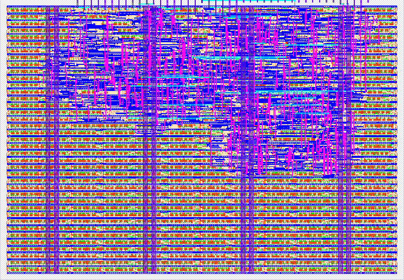
Created in the 1960s by Digital Equipment Corp., the PDP-8 has 4096 words of 12-bit wide memory. The design given here emulates a subset of PDP-8 instructions. It was inspired by Chapter 11 of my book, Verilog Digital Computer Design: Algorithms into Hardware, Prentice Hall, 1998, using a tool called Verilog Implicit to One-hot (VITO, see http://www.verilogvito.com/). VITO generated src/spdp7vv.v from a behaviorial (implicit-style) state machine shown at the bottom in the comments.
For simplicity and to fit within the pin count of Tiny Tapeout, memory size is reduced to 128 words (7-bit address, ma), and the data to and from memory is accessed one bit per clock cycle. Because of this serial operation, the bit address (ba) within the word must also be output (an extra 4 bits).
The only register in the PDP-8 is the ACcumulator and its one-bit extension called the LINK. The verilog treats this as a single 13-bit register, lac. Because of its 12-bit size, it is convenient to use octal notation. The instruction subset supported are: AND whose opcode is 0; Two Complement Add (TAD) whose opcode is octal 1; Increment and Skip if Zero (ISZ) whose opcode is 2; Deposit and Clear AC (DCA) whose opcode is 3; JMP whose opcode is 5; and microinstructions whose opcode is 7: group 1 (CLA, CLL, CMA, CML and IAC) and group 2 (conditional and halt). Only direct addressing is implemented. As this code came from a textbook example, other PDP-8 instructions and addressing modes were unimplemented and left as exercises. The actual PDP-8 had 12 switches to establish the initial program counter (pc); here because of pin count limitations the program must start at octal address 100.
How to test
It takes a special script to emulate the serial memory that contains the software and data which the fabricated CPU will operate on. There are verilog testbenchs (src/spdp7t0.v, src/spdp2t0.v andsrc/spdp2t0.v) that illustrate how to do this using a local verilog simulator, like iverilog. I used many similar testbenches when I was writing chapter 11, which makes me confident this design functions correctly.
To test the hardened design or the fabricated chip, such test code needs to be in python, as in test/test.py. I believe a slight variation of this will work with the fabricated chip. One example program in test.py has a CLA CLL (7300), TAD of data at 104 (1104), DCA this to 105 (3105) and HLT (7402). Another uses ISZ in a loop to compute 7*8.
I had some difficulty translating the verilog testbench to cocotb. Although in actual hardware or in verilog simulation it is possible for ma and ba to be generated in the same cycle as membus responds back (through the ui_in port), I could not figure out how to make cocotb accomplish this. The most natural approach is
dut.ui_in.value = (contin<<1)|membus. I also tried dut.ui_in.setimmediatevalue((contin<<1)|membus) and await Timer(). The data in the CPU always lagged one cycle behind what was required.
So I just assumed we can treat this like a slow memory, and I changed the verilog for the CPU. I added extra wait states to the CPU, which allow test.py to succeed.
External hardware
The design in my book connected an actual 1-bit wide RAM chip to ma and ba with one bit going back to the CPU on membus (this worked without the extra wait states). Using this python testbench, it is not necessary to connect a physical RAM since the python code simulates the memory.
IO
| # | Input | Output | Bidirectional |
|---|---|---|---|
| 0 | membus | ma[0] | ba[0] |
| 1 | contin | ma[1] | ba[1] |
| 2 | ma[2] | ba[2] | |
| 3 | ma[3] | ba[3] | |
| 4 | ma[4] | mb | |
| 5 | ma[5] | write | |
| 6 | ma[6] | unused | |
| 7 | halt | unused |