965 Wave Generator
965 : Wave Generator

- Author: Michael Mayr
- Description: Generates various functions, such as a sine wave, a sawtooth wave, a triangular wave and a squared wave.
- GitHub repository
- Open in 3D viewer
- Clock: 0 Hz
How it works

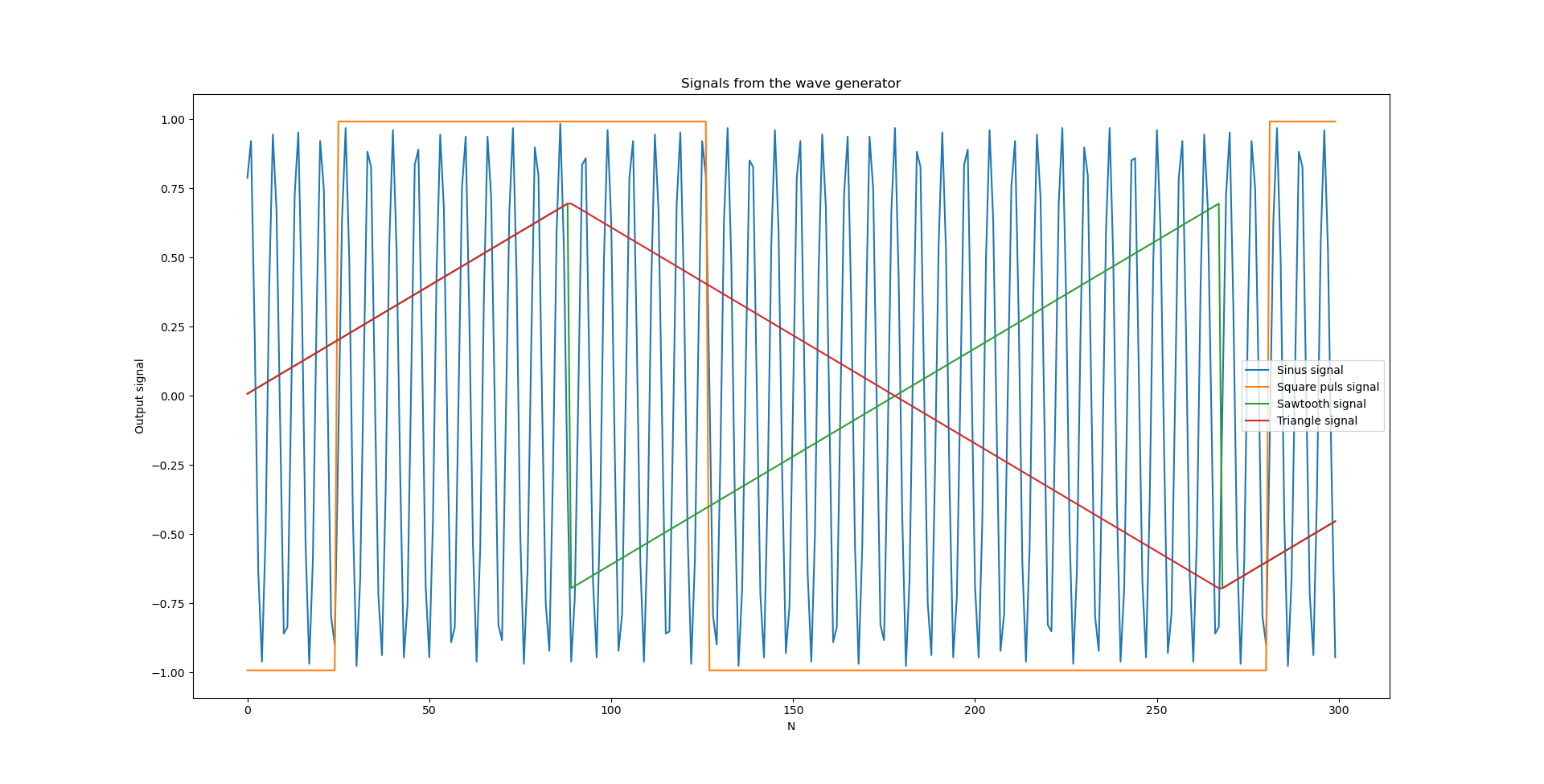
The Wave Generator is a project that deals with the generation of various signals. These signals are a sine function, a triangle function, a sawtooth function and a square pulse function. The desired function, which then provides the output value, can be selected using simple control signals.
Each calculated value is generated as a 2's complement in the fixed point system Q7 and then output accordingly either via the parallel or the serial interface. An SPI interface is used for the serial output, but this can only write and not read. However, this makes it possible to connect a DAC to the wave generator in order to convert the digital signals into analogue signals.
In general, the implemented signals can be influenced by three parameters:
- due to the internal clock frequency $f_{clk}$
- by the phase parameter
- by the amplitude parameter
These three parameters allow these signals to be flexibly configured in terms of their respective properties. Depending on the type of signal, however, certain restrictions must be taken into account for the parameters. These restrictions are then described in the respective section for the corresponding signal.
In addition, the sampling frequency $f_{s}$ is linked to the internal clock frequency $f_{clk}$ of the system by a factor of 40. A value therefore requires 40 clock pulses to be calculated and output via the serial interface. This results in the following relationship: $f_s = \frac{f_{clk}}{40}$. The maximum internal clock frequency $f_{clk}$ is $66\text{ MHz}$ and therefore the maximum sampling frequency $f_{s}$ is $1.65 \text{ MHz}$.
Inputs and outputs
The Wave Generator uses all 24 digital pins. The input pins are described in the pinout section. These 8 input pins add up to the bit vector parameter. This is required to set the phase and amplitude, as the respective value is applied to it as a 2's complement in the fixed-point system Q7. The bidirectional pins "set phase" and "set amplitude" are used to adopt this value as the phase value or amplitude value in the chip.
The current value is output in parallel form on the output wave pins and in serial form on the SPI pins. The SPI pins have the same names as defined in the standard, with the exception that the input pin MISO is missing. This is not required due to the pure data generation.
The bit vector wavefrom (see pinout section) is used to select the desired function. The desired function then results depending on the bit pattern:
- 00: Sine wave
- 01: Square puls wave
- 10: Sawtooth wave
- 11: Triangular wave
The value generation can be stopped by the pin enable (see pinout section) with a LOW level and continued with a HIGH level.
Sine wave
The sine wave is generated using a Cordic algorithm, as shown in the below figure. This Cordic algorithm is used in the mode rotation and with the coordinate system circular. The following function is implemented in the Cordic algorithm: $x_n = x_0 \cos(z_0) - y_0 \sin(z_0)$ $y_n = y_0 \cos(z_0) + x_0 \sin(z_0)$ To generate a sine wave from this formula, $y_0$ must be set to 0 and $x_0$ must be loaded with the desired amplitude. The current phase $z_0$ of the sine wave is calculated in advance by a phase accumulator. This then transfers its current phase value to the Z input of the Cordic algorithm. This allows the Cordic algorithm to generate a sine wave at the Y output, which is then subsequently output.
Due to a property of the Cordic algorithm, the amplitude parameter must be scaled by a factor $k$ before loading into the chip. This factor $k$ has a value of $0.6073$. This prevents an overflow in the Q7 format and the correct values are calculated by the algorithm.
This results in the following formulae for the parameters: $ \text{Amplitude parameter} = k A$ $\text{Phase parameter} = \frac{2f}{f_s}$ Where $A \in [-1+2^{-7}, 1-2^{-7}]$ is the desired amplitude and $f \in (0, \frac{f_s}{2}]$ is the desired frequency.

Square pulse wave
The square pulse wave is again calculated with a phase accumulator and a threshold dectection unit (see figure below). The phase accumulator generates a sawtooth function $x[n]$, where the difference between one value and its subsequent value is the phase parameter. An exception occurs in the case of an overflow. In this case, the difference is much greater, as the value moves to the negative end of the number format. This generated value is then compared with the current amplitude parameter. In this case, the amplitude parameter is a threshold parameter. The output is then generated according to the following principle: If $x[n]$ is greater than the amplitude parameter, $y[n]$ has the value $1-2^{-7}$. Conversely, if $x[n]$ is less than or equal to the amplitude parameter, $y[n]$ becomes $-1+2^{-7}$.
The following formulae are required for the parameters: $ \text{Amplitude parameter} = 1-2^{-7} - (2-2^{-7})\frac{T_{on}}{T}$ $\text{Phase parameter} = \frac{2-2^{-7}}{T f_s}$ Where $T > \frac{1}{f_s}$ is the desired period duration and $T_{on} \in (0, T)$ is the desired pulse width.

Sawtooth wave
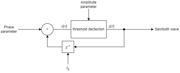
The sawtooth wave is basically generated with a phase accumulator (see figure below). The only difference is that $y[n]$ is fed back instead of $x[n]$. This makes it possible to generate a sawtooth function with a specific amplitude value. The threshold dectection unit thus ensures that the function remains in the range from minus amplitude parameter to amplitude parameter. To do this, $x[n]$ is checked and if this value is greater than the amplitude parameter, $y[n]$ is set to the negative value of the amplitude parameter. If this does not occur, $x[n]$ becomes $y[n]$.
The following formulae are required for the parameters: $ \text{Amplitude parameter} = A$ $\text{Phase parameter} = 2 A\frac{f}{f_s}$ Where $A \in [-1+2^{-7}, 1-2^{-7}]$ is the desired amplitude and $f \in (0, \frac{f_s}{2}]$ is the desired frequency.

Triangle wave
With the triangle wave, the current value is taken from the sawtooth wave and with every second overflow, therefore a change from a positive value to a negative value (see figure below), the output value is multiplied by -1.
The following formulas are required for the parameters: $ \text{Amplitude parameter} = A$ $\text{Phase parameter} = 4 A\frac{f}{f_s}$

SPI Interface
The calculated value is output serially via the SPI interface. The below timing diagram is used for this purpose. SPI is used in this project with CPOL=0 and CPHA=0. The SPI CLK requires 4 cycles of $f_{clk}$ for one cycle. The other properties can be taken from the timing diagram.

How to test
The following procedure is required to generate the desired wave:
- Initialisation
- Reset the device.
- The enable pin should be connected to LOW.
- Choose the desired wave
- Set the code for the desired wave on the waveform pins.
- Calculate the amplitude and the phase parameter with the formulars form the above sections.
- Set amplitude parameter
- Load the calculated results on the parameter pins
- Then send a puls to the set amplitude pin
- Set phase parameter
- Load the calculated results on the parameter pins
- Then send a puls to the set phase pin
- Enable the output generation
- The enable pin should be connected to HIGH.
- Now the chip generates the desired wave and output the values on the parallel and serial interface.
External hardware
Through the SPI interface it is possible to get an analogue signal through a suitable DAC. However, this DAC must fulfill the requirements of the SPI interface.
IO
| # | Input | Output | Bidirectional |
|---|---|---|---|
| 0 | parameter bit 0 (LSB) | output wave bit 0 | (input) enable pin |
| 1 | parameter bit 1 | output wave bit 1 | (input) waveform bit 0 pin |
| 2 | parameter bit 2 | output wave bit 2 | (input) waveform bit 1 pin |
| 3 | parameter bit 3 | output wave bit 3 | (input) set phase pin |
| 4 | parameter bit 4 | output wave bit 4 | (input) set amplitude pin |
| 5 | parameter bit 5 | output wave bit 5 | (output) spi cs pin |
| 6 | parameter bit 6 | output wave bit 6 | (output) spi mosi pin |
| 7 | parameter bit 7 (MSB) | output wave bit 7 | (output) spi clk pin |