492 TT06 Grab Bag
492 : TT06 Grab Bag
- Author: algofoogle (Anton Maurovic)
- Description: A few analog/mixed-signal experiments with a 24-bit VGA pattern generator as the highlight
- GitHub repository
- Open in 3D viewer
- Clock: 25000000 Hz
- Feedback: ✅ 2
What is this thing?
A simple analog/mixed-signal project I created in the 1st round of Matt Venn's Zero to ASIC Analog Course beta. This design has been demonstrated to work in silicon. For silicon test results, see my journal entry: https://algo.org/journal/0226
The design comprises:
- Simple CMOS inverter. That was my very first custom layout attempt.
- Digital block generating a few basic 24b-colour (RGB888) VGA test patterns.
- Analog RGB out (digital block VGA outputs via 3x 8-bit R2R DACs).
- An extra 4-bit R2R DAC.
VGA test pattern outputs
The design's main purpose is to generate VGA test patterns that were hoped to look as good as these simulations:

The left-hand pretty pattern is "MODE_XORS" (ui_in==8'b0011_0000) while the right-hand gradients pattern is "MODE_RAMP" (ui_in==8'b0001_0000).
Notice there is some horizontal smearing (more exaggerated in the right-hand image of the red/green mixes).
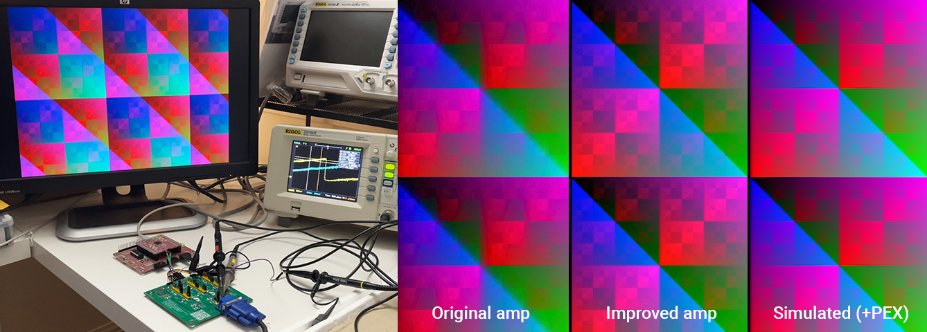
Actual results from silicon testing (seen above) are pleasing.
CMOS inverter
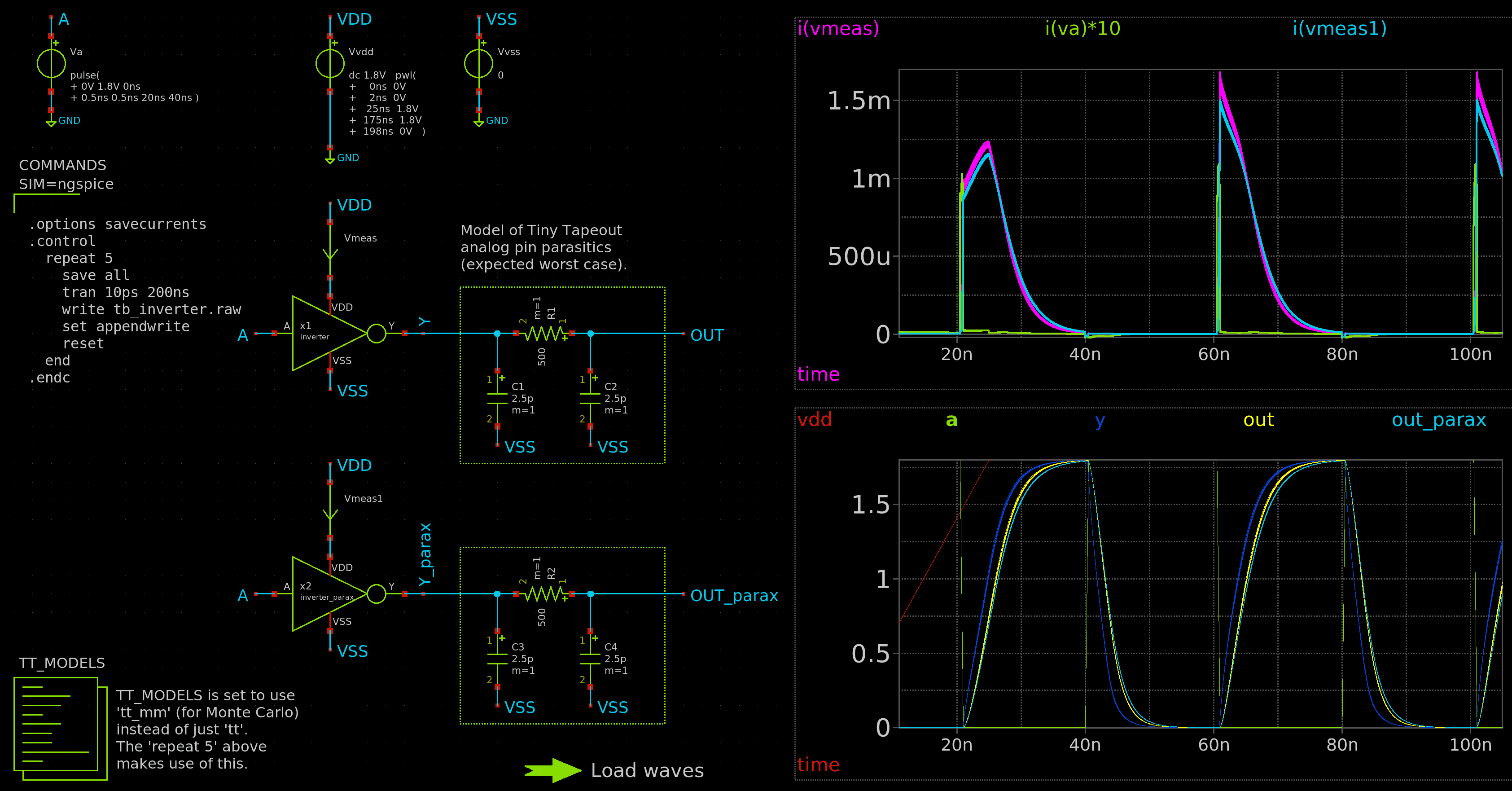
Pretty simple:
- Its input is
uio_in[7](bidir 7). - Its output goes to two places:
ua[3](analog) anduio_out[2](digital). - I'd expect its digital out performance to be better: the TT digital mux has more buffering & less loading than the TT analog mux.
The graphs accompanying the schematics simulate analog out is expected to be stable (enough) within 10ns; relatively poor performance characteristic of the TT analog mux loading. I expect bigger transistors could drive this harder and make it faster.
Extra 4-bit R2R
4th instance of my 8-bit R2R DAC cell grounds the 4 LSB, connecting the 4 MSB to spare bidir inputs (uio_in[6:4]) with DAC output via ua[4].
How it works
TBC!
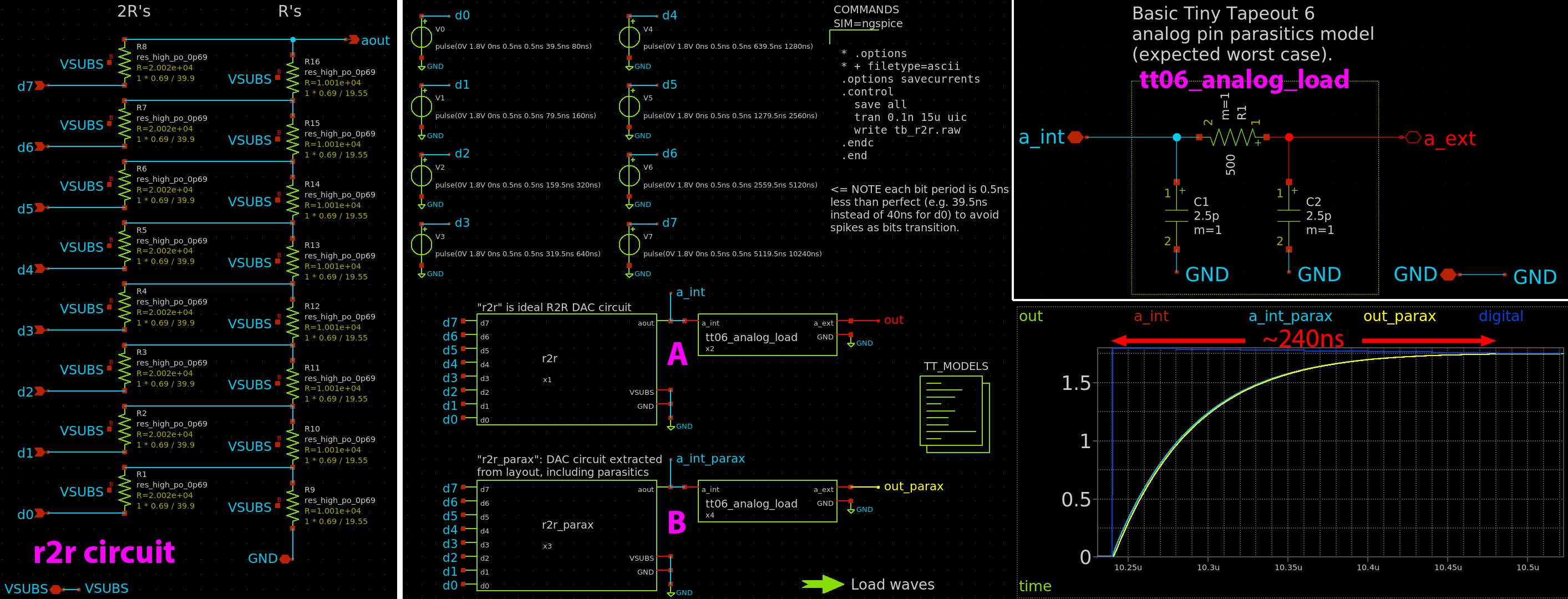
The internal R2R DACs for each of the RGB outputs just go directly (unbuffered) to the analog output pins, where they are subject to the loading of the TT06 analog mux (estimated to be about 500Ω and 5pF). This combination means their slew rate was expected to be pretty bad (at least by VGA timing standards): On the order of 240~360ns (or 6~9 horizontal pixels) going from 0V to full 1.8V. In the chips I received, it was a little better than that.
In a future design I plan to implement better internal buffering to help mitigate some of the TT analog mux load.
Select from a few simple test patterns in the VGA controller by having different ui_in values asserted while coming out of reset. the VGA controller digital block generates 8-bit digital outputs per each of red, green, and blue channels. These go into 3 basic RDACs to generate analog voltage outputs on ua[2:0] ({B,G,R}) in the range 0-1.8V (probably ~10kΩ impedance).
How to test
TBC!
- Supply a 25MHz clock
- Set
ui_into8'b0001_0000 - Assert reset -- NOTE: I didn't put a synchroniser on it, so it might (?) do a dirty reset -- if that happens, it could be worked around by slowly/manually clocking around the reset pulse, I guess.
- With a scope, trigger on the
uo_out[3]rising edge (VSYNC) and hopefully seeua[0]ramp from 0V to 1.8V within 10.24us - With this mode (as selected in step 2 above),
ua[1]will also ramp, but per line (instead of per pixel), as willua[2](per frame). - For the pretty XORs pattern, set
ui_into8'b0011_0000and assert reset again.
NOTE: For actual VGA output, you need the VSYNC and HSYNC signals (connecting them each with a 1kΩ resistor in series with their respective VGA cable connection should do). You will almost certainly need some sort of output buffering between this design and a VGA display, because the design outputs a high-impedance (~10kΩ but maybe a little worse) 0~1.8V range, while a VGA display expects 0~0.7V at 75Ω. See https://algo.org/pcb/tt06i for an example board that covers all this.
Other notes for testing:
- Digital block's mode selection is asserted via
ui_induring reset - For safety, initial test should be done with no analog output loading, and with all of
ui_inpulled low (which selects pass-thru mode AND ensures all DAC inputs internally are low, so hopefully no current). - RGB222 digital outputs compatible with the Tiny VGA PMOD.
External hardware
This is if you want to see an actual analog VGA display:
- 10MHz-capable (or better; preferably 25MHz) opamps on each of the R, G, B outputs, to both make them into low-impedance (matching 75Ω typical VGA termination), and also to level-shift from 0~1.8V to 0~0.7V. See https://algo.org/pcb/tt06i for an example "interposer board" (aka "sandwich board") which uses an OPA3355 video op-amp circuit with VGA connector, and is intended to sit between the TT06 chip's breakout board (aka "carrier") and the TT06 demo board.
- Optionally the Tiny VGA PMOD plugged into the dedicated output port (
uo_out).
IO
| # | Input | Output | Bidirectional |
|---|---|---|---|
| 0 | mode[0] / dac_in[0] | r7 | vblank_out |
| 1 | mode[1] / dac_in[1] | g7 | hblank_out |
| 2 | mode[2] / dac_in[2] | b7 | inv_dout |
| 3 | mode[3] / dac_in[3] | vsync | dac4_in[4] |
| 4 | mode[4] / dac_in[4] | r6 | dac4_in[5] |
| 5 | mode[5] / dac_in[5] | g6 | dac4_in[6] |
| 6 | mode[6] / dac_in[6] | b6 | dac4_in[7] |
| 7 | mode[7] / dac_in[7] | hsync | inv_in |
Analog pins
ua | PCB Pin | Internal index | Description |
|---|---|---|---|
| 0 | A5 | 5 | r_out |
| 1 | A0 | 0 | g_out |
| 2 | A4 | 4 | b_out |
| 3 | A1 | 1 | inv_aout |
| 4 | A3 | 3 | dac4_aout |
| 5 | A2 | 2 |
User feedback
- smunaut: I just looked at the behavior with ui=0x10 and the analog outpus ua[2:0] were as expected.
- algofoogle👑: Works better than expected! Vivid VGA images with high colour resolution. For a quick test: Plug in a Tiny VGA PMOD (on uo_out port), apply a 25MHz clock, set ui_in=0x30, and reset. For proper analog output testing, you'll need external buffers (i.e. op-amps) -- see the link to my testing notes and a board design for this. Link for more details