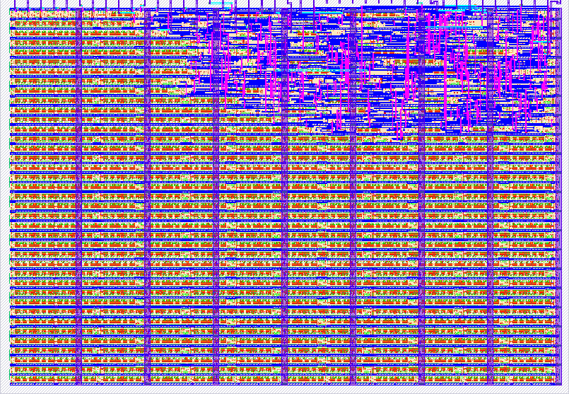
558 8-bit DEM R2R DAC
558 : 8-bit DEM R2R DAC

- Author: Eric Fogleman
- Description: 8-bit segmented mismatch-shaping R2R DAC
- GitHub repository
- Open in 3D viewer
- Clock: 10000000 Hz
Operation
This design implements a linear 8-bit DAC suitable for dc and low-frequency inputs. An analog voltage is produced by connecting the encoder's outputs to a modified R-2R ladder on the PCB (see External Hardware). It achieves high-linearity by using segmented mismatch-shaping, so the DAC does not require matched resistors. The encoder provides 1st order mismatch and quantization noise shaping. With a clock frequency of 6.144 MHz and a lowpass filter corner of 24 kHz, the oversampling ratio (OSR) is 256.
Error due to resistor mismatch appears at the output as 1st-order highpass shaped noise. The encoder also reduces the bit-width from 8-bits, and quantization error is also 1st-order highpass shaped. Thus, with passive filtering, a linear, low-noise dc output can be achieved. The theory behind this encoder is described in: A. Fishov, E. Fogleman, E. Siragusa, I. Galton, "Segmented Mismatch-Shaping D/A Conversion", IEEE International Symposium on Circuits and Systems (ISCAS), 2002
Ideally, this encoder would be buffered through a clean analog supply and retimed to reduce glitches on output transitions. However, reasonable performance should be possible driving the resistor ladder directly from the encoder through the IO supply.
How to test
DAC input data is provided through ui_in[7:0], and the encoder uses the project clock for mismatch shaping. Clock frequencies in the range of 1-10 MHz are reasonable. Higher clock frequency increases the OSR but may increase glitch error. The encoder output is uo_out[7:0], and it can be reconstructed by summing the bits with the following weights:
out = 8*(uo_out[7]+uo_out[6]) + 4*(uo_out[5]+uo_out[4]) + 2*(uo_out[3]+uo_out[2]) + uo_out[1]+uo_out[0]
The resistor ladder shown below sums the outputs with this weighting. Any output network that can create this weighting will work.

The DAC is free-running off the project clock, and inputs appear at the output immediately after passing through a pair of clock sync registers. A simple dc test can be performed using the input DIP switches and the resistor ladder. It is possible to input dynamic waveforms from the microcontroller as well.
The encoder has four modes of operation determined by uio_in[1:0]:
- 3: 1st order mismatch-shaping with dither
- 2: randomization (flat spectral shaping)
- 1: 1st order shaping, no dither
- 0: static encoding (no linearization)
External hardware
Technically, this is a mismatch shaping DAC encoder. For a high-performance DAC, it is best to use a precision reference voltage and a clean clock source for edge retiming. However, it is possible to connect the encoder directly to a resistor ladder. In this case, the digital IO supply acts as the DAC's reference voltage, and timing skews between the uo_out bits may impact performance.
An external resistor ladder is required to create the analog output voltage, and a capacitor is required to filter high-frequency noise. The termination resistors are placed at the ends of the ladder to ensure that each section has nominally identical load resistance.
The suggested unit R value is 10 kOhm. The equivalent output resistance of the network at v_out is 10 kOhm. A 680 pF output capacitor provides a 23 kHz lowpass corner. With this choice of R, the minimum load resistance on each uo_out pin is 60 kOhm, and the driver will source a maximum of 55 uA at 3.3 V.
IO
| # | Input | Output | Bidirectional |
|---|---|---|---|
| 0 | d_in[0] | d_out_0[0] | en_enc |
| 1 | d_in[1] | d_out_0[1] | en_dith |
| 2 | d_in[2] | d_out_1[0] | |
| 3 | d_in[3] | d_out_1[1] | |
| 4 | d_in[4] | d_out_2[0] | |
| 5 | d_in[5] | d_out_2[1] | |
| 6 | d_in[6] | d_out_3[0] | |
| 7 | d_in[8] | d_out_3[1] | ena_and_rst_n |