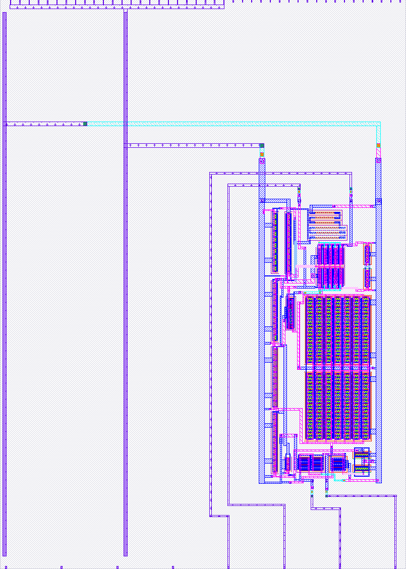
233 VCII
233 : VCII

- Author: Alfiero Leoni
- Description: Simple Voltage Conveyor
- GitHub repository
- Open in 3D viewer
- Clock: 0 Hz
How it works
The VCII (second generation Voltage Conveyor) is an analog block that has a low impedance current input pin (y), a high-impedance current output pin (x) and a low impedance output voltage pin (z) plus a reference voltage input pin (Ref) to provide the virtual ground reference for the circuit, behing used in single supply (for this design, ref is 0.9 V to be provided with a power supply). The VCII presents to main parameters: alpha and beta. Beta is the current gain, so placing a resisntance between x and ref and injecting a current in y, we should have that I(x) = betaI(Y). Aplha is the voltage gain, i.e. the voltage produced at the node x due to the current flowing will be amplified in z. The relationship is V(z)=alphaV(x). In this design, aplha and beta should be equal to 1, more or less.
How to test
The VCII could be tested in TIA (transimpedance amplifier) configuration. A current should be injected into the y pin (if a current source is not available, a big resistor can be used in serias to a voltage supply) of few uA. Then an external resistor should be connected between x and Vref. The resistor will set the TIA gain e.g. a resistor of 10K with an input sine current of 2uA pp should produce an output sine voltage of 20 mVpp to the z pin.
External hardware
The transipedance gain resistor, oscilloscope, power supplies
IO
| # | Input | Output | Bidirectional |
|---|---|---|---|
| 0 | |||
| 1 | |||
| 2 | |||
| 3 | |||
| 4 | |||
| 5 | |||
| 6 | |||
| 7 |
Analog pins
ua | PCB Pin | Internal index | Description |
|---|---|---|---|
| 0 | A4 | 4 | output |
| 1 | A1 | 1 | output |
| 2 | A3 | 3 | input |
| 3 | A2 | 2 | input |