231 TT06 8-bit SAR ADC
231 : TT06 8-bit SAR ADC

- Author: Carsten Wulff
- Description: 8-bit Successive Approximation Register ADC
- GitHub repository
- Open in 3D viewer
- Clock: 4000000 Hz
- Feedback: ✅ 3
Who
Carsten Wulff [email protected]
Why
Many years ago I made a compiler, and a state-of-the-art compiled ADC in 28 nm FDSOI, described in A Compiled 9-bit 20-MS/s 3.5-fJ/conv.step SAR ADC in 28-nm FDSOI for Bluetooth Low Energy Receivers.
Since then, I've ported the ADC to multiple closed PDKs (22 nm FDSOI, 22 nm, 28 nm, 55 nm, 65 nm and 130nm). A while ago I ported the SAR ADC to Skywater 130nm SUN_SAR9B_SKY130NM.
The fact that Tiny Tapeout now includes analog possibility inspired me to try and see if I could fit the SAR into the Tiny Tapeout area. The original 9-bit ADC did not fit, so I had to reduce it to 8-bit.
How to test
Apply a differential voltage with a common mode of around VDD/2 to ua[1] and ua[0]. If you want to measure the offset and noise of the ADC then connect ua[1] to ua[0] and provide 0.9 V to both.
A common mode of 0 V will not work. The comparator will not make a decision in time, and the asynchronous clock generation loop will be to slow.
Apply a 4 MHz clock to clk. Typical corner should be able to run faster.
Set ui_in[0] high to enable the ADC
The uo_out[7:0] is two's complement digital output. The MSB is [7].
The ADC will open the input switches to start sampling on the rising edge of the clock. The ADC will sample on the falling edge of the clock. When clock is low, then the asynchronous binary search algorithm tries to find the sampled analog input voltage, and convert the analog value to digital.
The uio_out[0] is the "done" signal from the asynchronous binary search algorithm. The digital outputs are sampled on the rising edge of this "done" signal.
If you want to capture the output of the ADC with a logic analyzer then I'd recommend you sample the digital outputs on the falling edge of the "done" signal.
Alternatively, you could sample on the rising edge of the clk, however, any insertion delay between the clk source and the ADC clk has to be taken into account.
If there is no "done" signal, then the clock is too fast, or the input common mode too low.
How it works
The differential input (ua[1:0]) is sampled onto a capacitor array. When the clk is high, the input switch is low resistance and the input voltage stabilizes on the capacitor array. When the clock goes low, the input switch will be high resistive, and the voltage on the capacitor array is sampled.
A strong arm comparator decides whether the differential voltage on the capacitor array is larger or smaller than zero.
Based on the comparator decision, parts of the capacitor array is switched from VPWR to VGND, or visa versa. A charge re-distribution will occur, which changes the differential voltage on the capacitor array.
A asynchronous custom digital logic performs a binary search to find the digital value.
The comparator input has the net name SARP and SARN. Observe those in a simulation to see how the SAR operates.
I would also recommend reading A Compiled 9-bit 20-MS/s 3.5-fJ/conv.step SAR ADC in 28-nm FDSOI for Bluetooth Low Energy Receivers, which explains the operation in detail. I've also added docs to sun_sar9b_sky130nm
Key parameters
| Parameter | Min | Typ | Max | Unit |
|---|---|---|---|---|
| Technology | SKY130A | |||
| AVDD | 1.7 | 1.8 | 1.9 | V |
| Temperature | -40 | 27 | 125 | C |
| Sampling frequency (CLK) | 4 | MHz | ||
| Average current VPWR | 48 | uA | ||
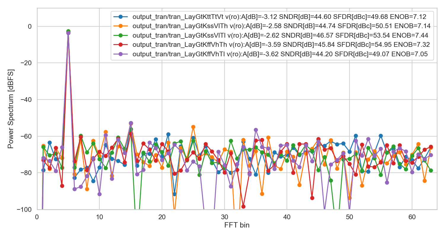
| SNDR_FS | 47.7 | dBFS | ||
| SFDR | 49.7 | dBc | ||
| ENOB_FS | 7.63 | bit |
Implementation
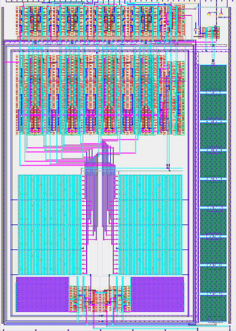
If you just want to see the layout, then go to http://analogicus.com/tt06-sar/
To have a look locally, do the commands below. I assume you have xschem, magic and the Skywater 130 nm PDK installed.
git clone --recursive [email protected]:wulffern/tt06-sar.git
cd tt06-sar/ip/tt06_sar_sky130nm/work/
xschem -b ../design/TT06_SAR_SKY130NM/tt_um_TT06_SAR_wulffern.sch &
magic ../design/TT06_SAR_SKY130NM/tt_um_TT06_SAR_wulffern.mag &
How to simulate
Install cicsim
python3 -m pip install cicsim
Navigate to the testbench and run a typical simulation (requires cicsim)
cd ip/tt06_sar_sky130nm/sim/TT06_SAR
make typical OPT="Debug"
The main testbench is ip/tt06_sar_sky130nm/sim/TT6_06/tran.spi
How to compile
The SAR ADC is made with ciccreator and cicpy.
The sources for the ADC are
ip/sun_sar9b_sky130nm/cic
├── ip.json                      # Object file, describes the object hierarchy of the circuits in the SAR
├── ip.spi                       # Spice file, describes the connectivity
├── capacitor.json               # Object file for capacitors
├── dmos_sky130nm_core.json      # Object file for transistors
└── sky130.tech                  # Technology file for Skywater 130 nm
The SAR is pre-compiled, so you don't really need to compile it. The compiled files are
in the ip/sun_sar9b_sky130nm/design/ directory.
If you want to try the compilation, then compile ip/ciccreator and install ip/cicpy, next
cd ip/sun_sar9b_sky130nm/work
make ip
Verification plan
Testbench folder ip/TT06_SAR_SKY130NM/sim/TT06_SAR/
| Purpose | Testbench | corner | Status | Notes |
|---|---|---|---|---|
| SNDR, SFDR, ENOB, active current | tran | tfs + C | OK | python3 tran.py <runfile> to plot FFT |
| tran | typ + RC | Not OK | RC extraction does not work yet | |
| Check power down after 2 sample, clock running | pwrdwn | typ | OK |
Results at TT06_SAR
Below is a Power Spectrum of a sinusoidal input signal

Known issues
| Nr | Issue | Solution | Discovery | Resolved |
|---|---|---|---|---|
| 1 | RC extraction removes coupling caps | 2024-04-13 |
1: RC extraction removes coupling caps
Extracting R and C seems to remove coupling caps, which removes both the cap in the bootstrapped switch, and the SAR. As a result, simulations don't work.
I make the RC extracted netlist with
cd ip/tt06_sar_sky130nm/work
make lper
In that command, I try to match the RC extracted netlist to the schematic netlist. First I remove all the parasitic Cs, the parasitic Rs and remove the R nets ( (t|n)\d+ ). The resulting RC extracted netlist is not LVS clean. The m3 resistors in BSSW have been removed.
I've also tried to change all parasitic resistors to 0.1 Ohm (make lowres),
but the simulation still does not work.
After a bit of digging it's clear that the cap between XCAP.B and XCAP.A in the BSSW is gone (it should be 0.3ish pF). There are almost no coupling caps, only caps to ground.
So I'm resonably sure it's not a real issue. It's a tool issue. Let's see when the IC comes back.
IO
| # | Input | Output | Bidirectional |
|---|---|---|---|
| 0 | Enable ADC | ADC LSB | Conversion Done |
| 1 | ADC MSB-6 | ||
| 2 | ADC MSB-5 | ||
| 3 | ADC MSB-4 | ||
| 4 | ADC MSB-3 | ||
| 5 | ADC MSB-2 | ||
| 6 | ADC MSB-1 | ||
| 7 | ADC MSB (two's complement) |
Analog pins
ua | PCB Pin | Internal index | Description |
|---|---|---|---|
| 0 | A5 | 5 | Negative ADC input |
| 1 | A0 | 0 | Positive ADC input |
User feedback
- smunaut: Works but both inputs needs to be above 0.6V for it to operate.
- rohanverma94: Used function generator as follows - CH1: sine(10 kHz), 500 mVpp, offset 900 mV, attached to A0 pin | CH2: sine(10 kHz), 500 mVpp, offset 900 mV, phase 180°, attached to A5 pin | Each pin swings from 0.65 V to 1.15 V | Differential voltage is 1 Vpp and Common-mode voltage as 0.9 V. | I can observe the varying output of ADC via commander app.
- wulffern👑: Works as expected (so far) Link for more details