How it works
The various registers used for a basic 8-bit CPU design.
Consists of a simple general purpose register, a memory address register, and an instruction register. The 3 registers are selected using the 6th and 7th uio pins.
| uio[7] |
uio[6] |
Selected Register |
| 0 |
0 |
General Purpose Register |
| 0 |
1 |
Memory Address Register |
| 1 |
0 |
Instruction Register |
Design Specifications
Instruction Register
| Label |
Input/Output |
Description |
| CLK [1 bit] |
Input |
Clock signal. Executes actions on rising edges. |
| W bus [8 bit] |
Input |
Takes 8 bits with the most significant 4 bits representing the opcode and the least significant 4 bits representing any other necessary value. Write them to the instruction register. |
| \L<sub>I</sub> [1 bit] |
Input |
Control signal that decides whether to read from the bus. |
| \E<sub>I</sub> [1 bit] |
Input |
Control signal that decides tri-state buffer output to bus (drive register value if enabled, Z if disabled). |
| CLR [1 bit] |
Input |
Clears the instruction register’s data. |
| Instruction register[3:0] [4 bit] |
Output |
Output to W bus |
| Instruction register[7:4] [4 bit] |
Output |
Output to controller/sequences |
Pinouts when instruction register is selected
| Test Input Name |
Description |
| clk |
CLK |
| ui_in[7:0] |
W bus |
| uio_in [4] |
\L<sub>I</sub> |
| uio_in [5] |
\E<sub>I</sub> |
| rst_n |
CLR |
| uio_out[3:0] |
Instruction register[7:4] |
| uo_out[3:0] |
Instruction register[3:0] |
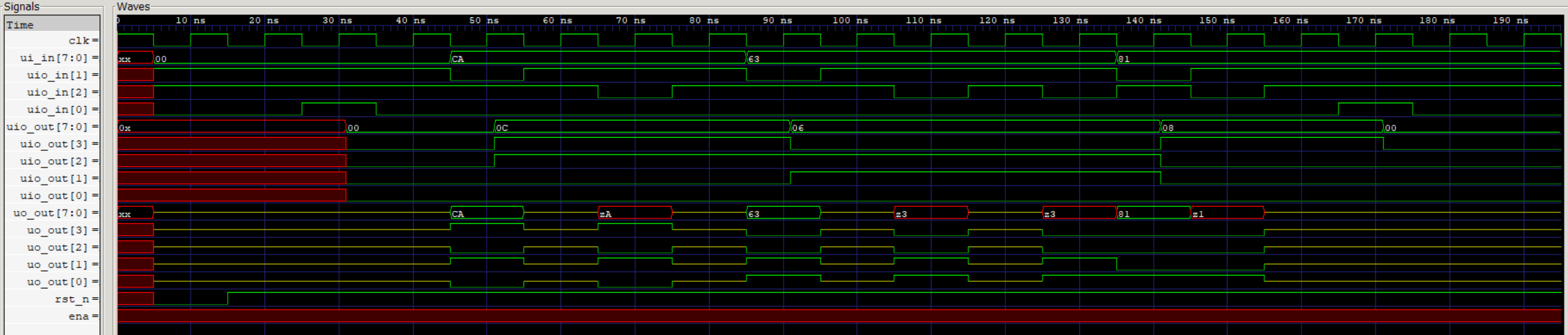
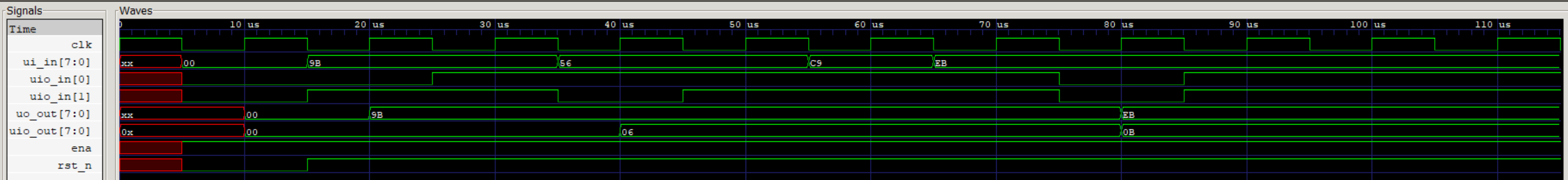
- Note: All simulations pictured in this document were run using a 10 ns clock. The actual design will have a 100 ns clock.
Test Input Connections (as seen in waveform)
| Test Input Name |
Description |
| clk |
CLK |
| ui_in[7:0] |
W bus |
| uio_in [1] |
\L<sub>I</sub> |
| uio_in [2] |
\E<sub>I</sub> |
| uio_in [0] |
CLR |
| uio_out[3:0] |
Instruction register[7:4] |
| uo_out[3:0] |
Instruction register[3:0] |
Output Register
| Label |
Input/Output |
Description |
| CLK [1 bit] |
Input |
Clock signal. Executes actions on rising edges. |
| W bus [8 bit] |
Input |
Data from the bus lines that are to be written to the Output register. |
| \L<sub>O</sub> [1 bit] |
Input |
Control signal that decides whether to read from the bus and load onto the output register. |
| Output register [8 bit] |
Output |
Register data that will be written to the binary display. |
Pinouts when output register is selected
| Test Input Name |
Description |
| clk |
CLK |
| ui_in[7:0] |
W bus |
| uio_in [4] |
\L<sub>O</sub> |
| uo_out[7:0] |
Output register |

Test Input Connections (as seen in waveform)
| Test Input Name |
Description |
| clk |
CLK |
| ui_in[7:0] |
W bus |
| uio_in [0] |
\L<sub>O</sub> |
| uo_out[7:0] |
Output register |
B Register
| Label |
Input/Output |
Description |
| CLK [1 bit] |
Input |
Clock signal. Executes actions on rising edges. |
| W bus [8 bit] |
Input |
Data from the bus lines that are to be written to the B register. |
| \L<sub>B</sub> [1 bit] |
Input |
Control signal that decides whether to read from the bus and load onto the B register. |
| B register [8 bit] |
Output |
Register data that will be written to adder/subtractor. |
Pinouts when b register is selected
| Test Input Name |
Description |
| clk |
CLK |
| ui_in[7:0] |
W bus |
| uio_in [4] |
\L<sub>B</sub> |
| uo_out[7:0] |
B register |
Test Input Connections (as seen in waveform)
| Test Input Name |
Description |
| clk |
CLK |
| ui_in[7:0] |
W bus |
| uio_in [0] |
\L<sub>B</sub> |
| uo_out[7:0] |
B register |
Input and MAR
| Label |
Input/Output |
Description |
| CLK [1 bit] |
Input |
Clock signal. Executes actions on rising edges. |
| W bus [8 bit] |
Input |
Data from the bus lines that are to be written either Input or MAR register. |
| \L<sub>MD</sub> [1 bit] |
Input |
Control signal that decides if W bus data is to be written to the Input register. Should not be active at the same time as the MA control signal. |
| \L<sub>MA</sub> [1 bit] |
Input |
Control signal that decides if W bus data is to be written to the MAR register. Should not be active at the same time as the MD control signal. |
| Input register [8 bit] |
Output |
Register data to be written to memory. |
| MAR [4 bit] |
Output |
Register data taken by RAM that controls where the data is to be written. |
Pinouts when input and mar register is selected
| Test Input Name |
Description |
| clk |
CLK |
| ui_in[7:0] |
W bus |
| uio_in [4] |
\L<sub>MD</sub> |
| uio_in [5] |
\L<sub>MA</sub> |
| uo_out[7:0] |
Input register |
| uio_out[3:0] |
MAR |
Test Input Connections (as seen in waveform)
| Test Input Name |
Description |
| clk |
CLK |
| ui_in[7:0] |
W bus |
| uio_in [0] |
\L<sub>MD</sub> |
| uio_in [1] |
\L<sub>MA</sub> |
| uo_out[7:0] |
Input register |
| uio_out[3:0] |
MAR |