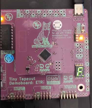
352 Hardware Entropy Explorer: UART/SPI TRNG and PUF
352 : Hardware Entropy Explorer: UART/SPI TRNG and PUF
- Author: gojimmypi
- Description: UART/SPI-controlled ASIC lab for exploring true-random number generation and PUF-style hardware entropy sources.
- GitHub repository
- Open in 3D viewer
- Clock: 25000000 Hz
How it works
A ring oscillator is implemented at the core of this project as an entropy source for a TRNG (True Hardware Random Number Generator).
This project exposes a UART-controlled interface to a ring-oscillator-based entropy source. A host such as a PC, ESP32, or test script can send simple ASCII commands over UART to configure internal registers, control the oscillator network, and read back raw entropy samples.
At a high level:
- A bank of ring oscillators generates jitter-based entropy
- A sampling clock (controlled by a divider) captures this behavior
- Control and configuration are managed through memory-mapped registers
- Data and status are read back over the same UART interface
Why? The National Institute of Standards and Technology (NIST) notes that random numbers are essential for cryptographic and security applications, and that cryptography makes extensive use of random numbers and random bits, particularly for generating cryptographic keying material.
See presentations:
SPI vs JTAG Special Note
JTAG is experimental only.
| Build / board | Physical setting | ui_in[4] |
debug_is_jtag |
Active interface |
|---|---|---|---|---|
| TT Demoboard | INPUT SW4/IN4 up/off |
0 |
0 |
SPI |
| TT Demoboard | INPUT SW4/IN4 down/on |
1 |
1 |
JTAG |
| ULX3S | gp4 high / unconnected pull-up |
1 |
0 |
SPI |
| ULX3S | gp4 pulled low |
0 |
1 |
JTAG |
For additional related information:
https://gojimmypi.github.io/trng/
https://gojimmypi.github.io/tinytapeout/
External Hardware
It can be helpful to have a TTY-UART USB adapter on hand to interact with the FSM and TRNG on the FPGA or ASIC. This can be used to send commands and read responses from the FSM and TRNG.
Most of the scripts to test assume the external UART. Testing and interactive commands could still be entered via the TT prompt.
FPGA Tests
This project can be tested on an FPGA such as these examples:
- Tiny Tapeout FPGA Development Kit Demoboard in the
ice40directory. - ULX3S ECP5 + ESP32 FPGA Development Board in the
ulx3sdirectory, and ESP32 SPI Example.
Note that the ring oscillators will not be implemented on the FPGA builds, rather a deterministic Linear-Feedback Shift Register (LFSR) is used in trng_lab_core.v to simulate the TRNG bitstream.
See the FPGA_NIST_PRNG_SOURCE and FPGA_BASIC_LFSR_RO_TAPS options in project_config.v
that are disabled for the TT build.
Commander App Tests
Use the commander.tinytapeout.com to connect to the tt-commander-app
How to test
The TT projects usually start in a reset mode = True. Connect to TT Breakout (or Demoboard) USB.
Once connected, there should be a Python REPL command prompt.
Don't confuse the TT board serial connection with the external UART.
Ensure all the dip input switches are in the up default (off) position.
Select the project, set the clock to 25 MHz, and reset. (see project_reset.py):
# select project and reset ttgf
tt.shuttle.tt_um_gojimmypi_ttgf_UART_FSM_TRNG_Lab.enable()

tt.clock_project_PWM(25000000)
tt.reset_project(True)
tt.reset_project(False)
Connect a UART terminal (e.g. PuTTY) to the TT Breakout (or Demoboard) I/O pins with the following connections:
- UART/TTY USB Tx to
IN3/Rx - UART/TTY USB Rx to
OUT4/Tx - GND to
GND
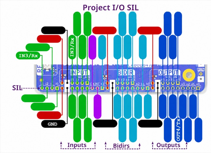
⚠ ** CAUTION: ** Pins are 3v3 and NOT expected to be 5v tolerant.
⚠ ** CAUTION: ** TT IO pins such as Tx and Rx are likely ** NOT ** tolerant to reversal. See TT Discord.
That's the same as shorting them. They're definitely not designed for it, but they won't die immediately either.
Note: IN3 and OUT4 are Tiny Tapeout logical signal names, not PMOD physical pin numbers. On the shown PMOD adapter:
in3is PMODIO4/physical pin 4.out4is PMODIO5/ physical pin 7.
Project config:
clock_hz: 25000000ininfo.yamldefine PROJECT_CLOCK_HZ 32'd25_000_000insrc/project_config.vdefine PROJECT_UART_BAUD 32'd115_200insrc/project_config.v
At a 25 MHz project clock with PROJECT_UART_BAUD = 115_200:
CLKS_PER_BIT = 25_000_000 / 115_200= 217- Terminal baud rate: 115,200
At a 50 MHz project clock, if the design is rebuilt with PROJECT_CLOCK_HZ = 50_000_000:
CLKS_PER_BIT = 50_000_000 / 115_200= 434- Terminal baud rate: 115,200
If the bitstream was built for 25 MHz but the board is actually clocked at 50 MHz, the effective UART baud rate doubles to approximately 230,400 baud.
Terminal session at 25 MHz clock is
- 115,200 baud
- 8 data bits
- No parity
- 1 Stop
- No flow control (Although the default XON/XOFF should also work, but ignored)
Or:
stty -F "$PORT" "$BAUD" cs8 -cstopb -parenb -ixon -ixoff -crtscts raw -echo min 0 time 5
Type V and press Enter to query the version string (if enabled in the build, on by default for TT).
Then you can send commands to configure the TRNG and read back entropy samples.
⚠ The TT Build is Case Sensitive. Although there are case-insensitive settings available for local FPGA builds, they have been disabled for TT ASIC due to observed increased slew and setup violations.
Type RD and press enter to view the Build Target ID. The expected value for GF180 ASIC is 42.
Send the appropriate commands to configure and read from the TRNG core. See Register Overview, below.
NIST Validation
NIST has a Resource for Random Bit Generation testing:
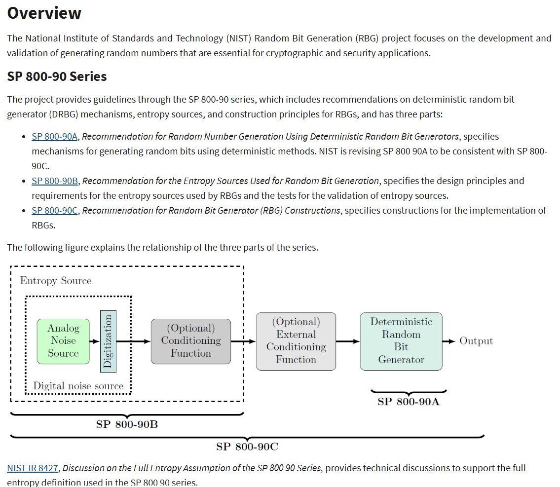
Image credit: screen snip from csrc.nist.gov/Projects/random-bit-generation
See the capture_trng_raw_uart.py
script to capture a binary file of random data from this project, large enough for 100 runs of 1,000,000-bit
NIST-style tests:
# WSL /dev/ttyS[n] == COM[n] on Windows, other Linux: /dev/ttyUSB[n], /dev/ttyACM[n], etc

./capture_trng_raw_uart.py  --port /dev/ttyS12  --bytes 16777216  --out trng_raw.bin
This script requires a build with TRNG_BINARY_STREAM enabled.
The raw output is intended for experimentation and characterization. It is not a certified cryptographic random number generator.
When the optional define TRNG_CONDITIONED_STREAM is used in project_config.v,
the conditioned output can be generated with the --conditioned option:
./capture_trng_raw_uart.py \
    --port /dev/ttyS12 \
    --bytes 16777216 \
    --out trng_conditioned.bin \
    --fast-baud \
    --conditioned
See also:
# The official STS package from NIST CSRC:
# https://csrc.nist.gov/CSRC/media/Projects/Random-Bit-Generation/documents/sts-2_1_2.zip

unzip sts-2_1_2.zip
cd sts-2.1.2
make

#
# or this UNOFFICIAL mirror:
# https://github.com/terrillmoore/NIST-Statistical-Test-Suite.git

cd NIST-Statistical-Test-Suite
./setup.sh
cd sts
make
For further testing information see NIST Random Bit Generation RBG - Guide to the Statistical Tests.
Quickstart Simulation
cd /mnt/c/workspace/ttgf-UART-FSM-TRNG-Lab/test

./my_test.sh

./jtag_test.sh
Quickstart Testing on TT Demoboard
If all the toolchains are installed:
cd /mnt/c/workspace/ttgf-UART-FSM-TRNG-Lab/ice40

source ./env_ice40.sh
./build_and_flash.sh
./project_reset.sh
./run_tests.sh
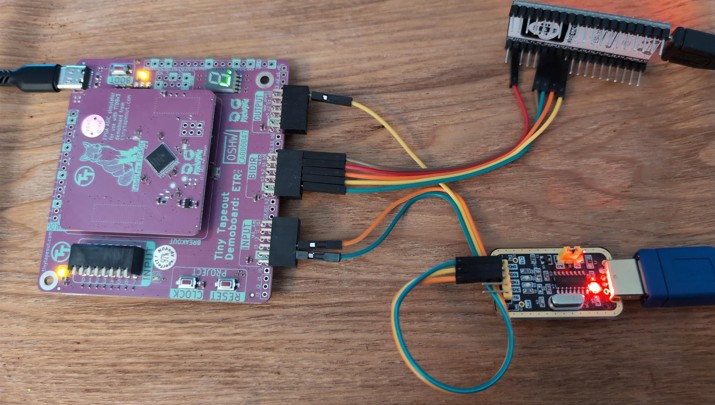
Sample Soft SPI connected to ESP32 and Soft UART connected to external USB/TTY UART.
Despite the "F" that may be repeatedly displayed on the 7-segment display during testing, that does not indicate failure:
From youtube.com/shorts/zFnfsl1DQHE
Quickstart Testing on ULX3S
See the [project]/ulx3s and [project]/test-hw directories.
ULX3S Connections
All pins are 3v3 and assumed to NOT be 5v tolerant.
Soft External UART
⚠ Do not connect to 5V TTY
GNDonJ1pin 4; Ground connection. Beware of adjacent3v3onJ1pins 1 and 2.GP0forRxonJ1pin 6 (connect to external USB/TTY UARTTx)GP1forTxonJ1pin 8 (connect to external USB/TTY UARTRx)
Soft SPI
Select SPI by leaving TT IN4 up/off, or leaving ULX3S gp4 high/unconnected/pull-up.
- For TT boards,
INPUTDip SwitchIN4up/off givesui_in[4] = 0, selecting SPI. - For ULX3S,
gp4high/unconnected/pull-up givesshared_spi_jtag_select = 1, selecting SPI.
Pins are already connected to the on-board ESP32 - but for debugging reference:
GNDonJ1pin 5; Ground connection. Beware of adjacent3v3onJ1pins 1 and 2.GN2-> (TTuio[0]) TMSGP2-> (TTuio[1]) TDIGN3<- (TTuio[2]) TDOGP3-> (TTuio[3]) TCK
See /ulx3s/ESP32/main/ulx3s_spi_lib.c
⚠ Do not accidentally wire ESP32 GPIO2 to PMOD GP2. GPIO2 goes to GN3, because it is MISO/TDO.
Also be careful around J1: use pin 5 GND, not the adjacent 3v3 pins 1/2.
ULX3S ESP32 SPI Pins
#define PIN_NUM_MISO        2
#define PIN_NUM_MOSI        15
#define PIN_NUM_CLK         14
#define PIN_NUM_CS          13
#define SPI_CLOCK_HZ        1000000
| ESP32 signal | ESP32 GPIO | TT/PMOD pin | TT signal | JTAG-style name | Direction | Wire |
|---|---|---|---|---|---|---|
PIN_NUM_CS |
GPIO13 | GN2 |
uio[0] |
TMS |
ESP32 -> TT | Brown |
PIN_NUM_MOSI |
GPIO15 | GP2 |
uio[1] |
TDI |
ESP32 -> TT | Red |
PIN_NUM_MISO |
GPIO2 | GN3 |
uio[2] |
TDO |
TT -> ESP32 | Orange |
PIN_NUM_CLK |
GPIO14 | GP3 |
uio[3] |
TCK |
ESP32 -> TT | Yellow |
GND |
ESP32 GND | J1 pin 5 |
GND |
- | common ground | Green |
Stand-alone ESP32 SPI Pins
⚠ Do not use these pins on the ULX3S ESP32.
Disable IS_ULX3S_ESP32 macro in ulx3s_spi_lib.c to use external stand-alone ESP32:
#define PIN_NUM_MISO        19
#define PIN_NUM_MOSI        23
#define PIN_NUM_CLK         18
#define PIN_NUM_CS          21
#define SPI_CLOCK_HZ        1000000
| ESP32 signal | ESP32 GPIO | TT/PMOD pin | TT signal | Direction | Wire |
|---|---|---|---|---|---|
PIN_NUM_CS |
GPIO21 | GN2 |
uio[0] / CS / TMS |
ESP32 -> TT | Brown |
PIN_NUM_MOSI |
GPIO23 | GP2 |
uio[1] / MOSI / TDI |
ESP32 -> TT | Red |
PIN_NUM_MISO |
GPIO19 | GN3 |
uio[2] / MISO / TDO |
TT -> ESP32 | Orange |
PIN_NUM_CLK |
GPIO18 | GP3 |
uio[3] / SCK / TCK |
ESP32 -> TT | Yellow |
GND |
ESP32 GND | J1 pin 5 |
GND |
common ground | Green |
Build and run tests from the ./test-hw directory.
cd /mnt/c/workspace/ttgf-UART-FSM-TRNG-Lab/test-hw

# may need to remove generated file
rm  ../src/_tt_fpga_top.v

# Edit board version as needed, tested on older v3.0.7:
./run_tests.sh  --with-build  --ulx3s-board-version v307  --ignore-combinational-warning  --no-warning-pause  --port /dev/ttyS12 --pause-for-test
Quickstart on ULX3S ESP32
The onboard ESP32 is pre-configured to work with this TT project. No external wiring is needed.
# [project]/ulx3s/ESP32
cd /mnt/c/workspace/ttgf-UART-FSM-TRNG-Lab/ulx3s/ESP32

PORT=/dev/ttyS3

idf.py -p $PORT -b 115200 flash
idf.py -p $PORT -b 115200 monitor
See also Comprehensive Testing below and the TT MicroPython SDK v3.
Register Overview
| Register | Description |
|---|---|
reg_ctrl |
Global control bits (enable, feature flags) |
reg_src |
Selects entropy source or oscillator group |
reg_div |
Clock divider controlling sampling rate |
reg_mode |
Operating mode configuration |
reg_oscen |
Bitmask enabling individual oscillators |
reg_status |
Status flags (data ready, internal state) |
reg_rawlo |
Low byte of raw sampled entropy |
reg_rawhi |
High byte of raw sampled entropy |
Key Concepts
-
Enable (
E)
Must typically be cleared (E0) before changing configuration, then set (E1) to run. -
Oscillator Control (
O)
Enables one or more ring oscillators. More oscillators can improve entropy but may affect stability. -
Sampling (
D)
The divider controls how frequently entropy is sampled. This impacts randomness quality and bias. -
Source Selection (
S)
Allows switching between different entropy paths or test modes (implementation-specific). -
Raw Data (
R6,R7)
Returns unprocessed entropy bytes. These are not whitened and may require post-processing.
Typical Flow
- Disable the core (
E0) - Configure source, divider, mode, and oscillators
- Enable the core (
E1) - Read entropy and status via
R6,R7,R5
This simple interface allows interactive exploration of TRNG behavior directly from a terminal.
UART TRNG Command Interface
All commands are ASCII and terminated with \r.
Responses are ASCII for normal register/configuration commands, typically:
R<n>=<value>
The optional Bxx raw stream command returns binary bytes and does not append OK<CR>.
Write Commands
| Cmd | Description |
|---|---|
E<n> |
Write enable bit (0=disable, 1=enable) |
S<n> |
Write source select |
V<n> |
Write control bit 1 |
W<n> |
Write control bit 2 |
D<hex> |
Write divider |
M<hex> |
Write mode |
O<hex> |
Write oscillator enable mask |
Special:
V\r-> returns version string (if enabled in build)
Read Commands
| Cmd | Description |
|---|---|
| R0 | Read reg_ctrl |
| R1 | Read reg_src |
| R2 | Read reg_div |
| R3 | Read reg_mode |
| R4 | Read reg_oscen |
| R5 | Read reg_status |
| R6 | Read reg_rawlo |
| R7 | Read reg_rawhi |
Examples
Enable and configure:
E0\r
V0\r
W0\r
S0\r
D10\r
M00\r
O01\r
E1\r
Read back registers:
R0\r -> R0=01
R2\r -> R2=10
R6\r -> R6=7B
R7\r -> R7=3C
Version query:
V\r -> Version x.x.x <date>
Binary raw stream, when enabled:
B10<CR> -> 16 raw binary bytes
B64<CR> -> 100 raw binary bytes
BFF<CR> -> 255 raw binary bytes
B00<CR> -> ?<CR>
The xx byte count is hexadecimal, not decimal.
Do not use a normal terminal to view Bxx output. The response may contain arbitrary byte values, including control characters. Use capture_trng_raw_uart.py or another binary-safe capture tool.
Notes
- Commands are stateful; configure with
E0before changes R6/R7provide raw entropy bytesOcontrols active oscillators (entropy source)Daffects sampling rate and bias
UART
Connect with your favorite terminal program such as putty.
For the ULX3S FPGA, the UART is connected to pins gp0 and gp1 The default baud rate is 115200.
See the default reference ULX3S ulx3s_v20.lpf restraint file.
The B11 (aka gp[0] or gp0) is Rx, to UART Tx.
The A10 (aka gp[1] or gp1) is Tx, to UART Rx.
# UART pins for testing

LOCATE COMP "uart_rx_pin" SITE "B11"; # formerly "gp[0]"; # J1_5+  GP0 PCLK
IOBUF PORT "uart_rx_pin" IO_TYPE=LVCMOS33;

LOCATE COMP "uart_tx_pin" SITE "A10"; # formerly "gp[1]"; # J1_7+  GP1 PCLK
IOBUF PORT "uart_tx_pin" IO_TYPE=LVCMOS33;
Comprehensive Testing
There are TT simulation tests and local ULX3S FPGA tests.
Set the TT_PROJECT_ROOT environment variable to the root of the project directory before running the tests or other scripts.
export TT_PROJECT_NAME="ttgf-UART-FSM-TRNG-Lab"
export TT_PROJECT_ROOT="/mnt/c/workspace/$TT_PROJECT_NAME"
Testing on the Tiny Tapeout FPGA Development Kit
See the overview video for the FPGA Development Kit.
Testing ULX3S / TT
First run this script in one bash terminal, note test pause "Press Enter to continue..." (see concurrent Testing ESP32, below)
cd "$TT_PROJECT_ROOT/test-hw"

./run_tests.sh  --with-build  --ulx3s-board-version v307  --ignore-combinational-warning  --no-warning-pause  --port /dev/ttyS12 --pause-for-test
Testing SPI with ESP32
The ULX3S has a built-in ESP32, but a standalone ESP32 can also be used to test the SPI interface.
Current testing scripts:
# change directory to your ESP-IDF directory:
cd /mnt/c/SysGCC/esp32-master/esp-idf/v5.5

source ./export.sh

cd "$TT_PROJECT_ROOT/ulx3s/ESP32"
idf.py build

idf.py -p /dev/ttyS3 -b 115200 flash

idf.py -p /dev/ttyS3 -b 115200 monitor
There should be output from the ESP32 showing the SPI transactions and register values. This can be used to verify that the SPI interface is working correctly and that the TRNG lab core is responding to commands. (See example output):
gojimmypi:/mnt/c/workspace/ttgf-UART-FSM-TRNG-Lab/ulx3s/ESP32
$ idf.py -p /dev/ttyS3 -b 115200 monitor
Executing action: monitor
Running idf_monitor in directory /mnt/c/workspace/ttgf-UART-FSM-TRNG-Lab/ulx3s/ESP32
Executing "/home/gojimmypi/.espressif/python_env/idf5.5_py3.10_env/bin/python /mnt/c/SysGCC/esp32-master/esp-idf/v5.5/tools/idf_monitor.py -p /dev/ttyS3 -b 115200 --toolchain-prefix xtensa-esp32-elf- --target esp32 --revision 0 /mnt/c/workspace/ttgf-UART-FSM-TRNG-Lab/ulx3s/ESP32/build/ulx3s_esp32.elf /mnt/c/workspace/ttgf-UART-FSM-TRNG-Lab/ulx3s/ESP32/build/bootloader/bootloader.elf -m '/home/gojimmypi/.espressif/python_env/idf5.5_py3.10_env/bin/python' '/mnt/c/SysGCC/esp32-master/esp-idf/v5.5/tools/idf.py' '-p' '/dev/ttyS3' '-b' '115200'"...
--- esp-idf-monitor 1.6.2 on /dev/ttyS3 115200
--- Quit: Ctrl+] | Menu: Ctrl+T | Help: Ctrl+T followed by Ctrl+H
I (13) boot: ESP-IDF v5.5 2nd stage bootloader

  [... snip. etc ... ]
I (350) main: SPI write mode: boot config once
I (350) ulx3s_spi: SPI regs: R0=00 R1=00 R2=10 R3=00 R4=01 R5=04 R6=3E R7=84 raw=0x843E status=0x04 src=0 div=0x10 mode=0x00 oscen=0x01
I (460) main: TRNG deterministic LFSR test
I (460) main: lfsr test sample 00: raw=0x7F2E status=0x00
I (460) main: lfsr test sample 01: raw=0x9F33 status=0x00


  [... snip. etc ... ]

I (740) ulx3s_spi: SPI regs: R0=00 R1=00 R2=10 R3=00 R4=01 R5=04 R6=3E R7=84 raw=0x843E status=0x04 src=0 div=0x10 mode=0x00 oscen=0x01
I (740) ulx3s_spi: SPI regs: R0=00 R1=00 R2=10 R3=00 R4=01 R5=04 R6=3E R7=84 raw=0x843E status=0x04 src=0 div=0x10 mode=0x00 oscen=0x01
If the ./run_tests.sh was left at the Press Enter to continue... prompt, press Enter to continue with the next set of tests.
The output should look something like this example:
Build PASSED
Flash...
Flashing file:
-rw-r--r-- 1 gojimmypi gojimmypi 294455 Jun  4 08:22 /mnt/c/workspace/ttgf-UART-FSM-TRNG-Lab/ulx3s/ulx3s.bit
ULX2S / ULX3S JTAG programmer v4.8 (git 96ebb45 built Oct  7 2020 22:42:00)
Copyright (C) Marko Zec, EMARD, gojimmypi, kost and contributors
Using USB cable: ULX3S FPGA 12K v3.0.3
Programming: 100%
Completed in 12.78 seconds.
/mnt/c/workspace/ttgf-UART-FSM-TRNG-Lab/test-hw
Press Enter to continue...

Skipping register reset. Use --reset-registers to start from configured defaults.

Running: version_if_present
Version probe response: b'Version 0.1.5d 6/3/2026\r'
PASS: Version command

  [... snip. etc ... ]
The continued output from the ESP32 in the separate TTY window should look something like this:
I (186760) ulx3s_spi: SPI regs: R0=06 R1=00 R2=10 R3=00 R4=01 R5=00 R6=00 R7=00 raw=0x0000 status=0x00 src=0 div=0x10 mode=0x00 oscen=0x01
I (187760) ulx3s_spi: SPI regs: R0=06 R1=00 R2=2A R3=5C R4=0F R5=00 R6=00 R7=00 raw=0x0000 status=0x00 src=0 div=0x2A mode=0x5C oscen=0x0F
I (188760) ulx3s_spi: SPI regs: R0=00 R1=00 R2=10 R3=00 R4=01 R5=04 R6=00 R7=00 raw=0x0000 status=0x04 src=0 div=0x10 mode=0x00 oscen=0x01
TT Simulation tests
Commit changes. See results in actions.
In particular, note the output of the gds workflow:
- Linter output
- Routing Stats
- Cell usage by Category
- Tiny Tapeout Precheck Results
- Viewer summary
Test on ULX3S FPGA
Build and flash the bitstream to the FPGA, then run the test script. The test script will print the output of the FSM and TRNG.
Test locally with ULX3S ECP5 FPGA in /ulx3s/ directory.
Example:
cd ulx3s

./ulx3s_build.sh
./ulx3s_flash.sh
Connect to the FPGA using a serial terminal (e.g., putty or minicom) to view the output of the FSM and TRNG.
Local Loopback Test
There are two loopback tests: a basic loopback test and a deep loopback test. The basic loopback test verifies that the UART is functioning correctly by sending data from the FPGA to the host and back. The deep loopback test verifies that the FSM and TRNG are functioning correctly by sending commands to the FPGA and reading the responses.
Basic Loopback Test
The basic loopback assigns Tx to Rx in top_ulx3s.v.
assign uart_tx_pin = uart_rx_sync;
All characters should be echoed back in the terminal when you type. This verifies that the UART is working correctly.
Sample loopback build defines FORCE_LOOPBACK=1 macro in ulx3s_build.sh:
./ulx3s_build.sh --loopback --ignore-combinational-warning --no-warning-pause
./ulx3s_flash.sh
Deep Loopback Test
./ulx3s_build.sh --deep-loopback --ignore-combinational-warning --no-warning-pause
./ulx3s_flash.sh
Extensive loopback tests
Additional loopback tests:
    # The safest test to start (default write_with_delay when --bulk not specified)
    python ./loopback_test.py --port $PORT -b 115200                  || exit 1

    echo "Test non-bulk mode, delay = 0.005"
    python ./loopback_test.py --port $PORT -b 115200 --tx-delay 0.005 || exit 1

    echo "Test non-bulk mode, delay = 0.001"
    python ./loopback_test.py --port $PORT -b 115200 --tx-delay 0.001 || exit 1

    echo "Test non-bulk mode, delay = 0.000"
    python ./loopback_test.py --port $PORT -b 115200 --tx-delay 0.000 || exit 1

    echo "Test bulk mode most challenging"
    python ./loopback_test.py --port $PORT -b 115200 --bulk           || exit 1
The run_tests.sh can be used to run the loopback tests with the appropriate flags:
cd "$TT_PROJECT_ROOT/test-hw

./run_tests.sh --with-build --ignore-combinational-warning --no-warning-pause --loopback
./run_tests.sh --with-build --ignore-combinational-warning --no-warning-pause --deep-loopback
./run_tests.sh --with-build --ignore-combinational-warning --no-warning-pause
Local Automated Hardware Operation Tests
Generic local hardware operation tests in /test-hw/.
- tt_uart_test.py - Python script to test the UART functionality of the FSM and TRNG on the ULX3S FPGA. It sends commands to the FPGA and reads the responses to verify correct operation.
- run_tests.sh - Shell script to run the hardware tests. It can be configured to build the FPGA bitstream, flash it to the FPGA, and run the Python test script.
cd test-hw

 ./run_tests.sh --with-build --ignore-combinational-warning --no-warning-pause
UART FSM TRNG Lab Datasheet
Document revision: 1.0.5
RTL revision string: Version 1.0.5 6/21/2026
Project family: Tiny Tapeout UART/SPI configurable TRNG experiment
Primary top modules: tt_um_gojimmypi_ttgf_UART_FSM_TRNG_Lab (conditional based on build)
License: Apache-2.0, as declared in the source files
1. Overview
The UART FSM TRNG Lab is a Tiny Tapeout compatible experimental random-number and entropy-source project. It exposes a small register bank through an ASCII UART command interface and, when enabled, an SPI mode 0 register-access interface. The design is intended for laboratory bring-up, education, FPGA validation, and ASIC ring-oscillator entropy experiments.
The core supports multiple sample sources:
- Deterministic LFSR source for repeatable tests
- Single ring-oscillator sample source
- XOR of multiple ring-oscillator sources
- Mixed source combining ring-oscillator and LFSR-derived state
The design is not a certified cryptographic random number generator. Raw output should be characterized, health-tested, and conditioned before use in security-sensitive systems.
2. Key Features
- Tiny Tapeout standard digital pin interface
- UART RX/TX control path using ASCII commands
- Optional SPI register-access slave
- SPI mode 0, MSB first
- Shared UART and SPI register bank
- 8-byte logical register map
- Configurable sample divider
- Selectable entropy/sample source
- Ring oscillator enable mask
- Deterministic single-step mode for test reproducibility
- Reset control through a configuration bit
- Default 25 MHz project clock
- Default 115200 baud UART
- ASIC real ring-oscillator path for selected PDK builds
- FPGA/simulation-safe LFSR tap substitute when real ring oscillators are disabled
3. Design Status and Intended Use
This block is intended as an experimental TRNG lab core. It is suitable for:
- Tiny Tapeout project demonstration
- FPGA bring-up on ULX3S or similar wrappers
- UART command parser testing
- SPI register interface testing
- Ring oscillator experimentation in supported ASIC flows
- Deterministic regression testing using the LFSR source
It is not, by itself, suitable as a drop-in cryptographic RNG. The raw output is unconditioned and no formal entropy claim is made in this datasheet.
4. Source Files
The main RTL files are:
| File | Purpose |
|---|---|
project.v |
Top-level Tiny Tapeout project wrapper and project feature defines |
project_config.v |
Project clock and UART baud configuration |
target_pdk.v |
PDK target selection |
tt_um_main.v |
Tiny Tapeout pin mapping and UART/SPI/TRNG integration |
UART/uart_rx_min.v |
Minimal UART receiver |
UART/uart_tx_min.v |
Minimal UART transmitter |
UART/uart_trng_ascii_core.v |
UART and TRNG integration core |
TRNG/trng_cfg_ascii_core.v |
ASCII command parser and register bank |
TRNG/trng_lab_core.v |
Experimental TRNG/lab source logic |
TRNG/trng_stub.v |
Stub/test TRNG replacement when the lab core is not enabled |
SPI/spi_slave.v |
SPI mode 0 register-access slave |
JTAG/jtag_core.v |
Optional JTAG-related logic |
5. Top-Level Parameters
| Parameter | Default | Description |
|---|---|---|
CLOCK_HZ |
25000000 |
Project clock frequency in Hz |
UART_BAUD |
115200 |
UART baud rate |
The source contains parameter checks that intentionally fail elaboration if either parameter is zero or if CLOCK_HZ / UART_BAUD would be zero.
The ULX3S_USE_GN12_50MHZ configuration path can set PROJECT_CLOCK_HZ to 50 MHz for the optional ULX3S gn12 clock path. Normal builds use the 25 MHz project clock.
6. Build-Time Feature Defines
| Define | Purpose |
|---|---|
UART_ENABLED |
Enables UART-related integration |
SPI_ENABLED |
Enables the SPI slave pin path |
SPI_REG_ACCESS |
Enables SPI access to the shared register bank |
TRNG_ENABLED |
Selects the TRNG lab core instead of the stub core |
JTAG_ENABLED |
Enables JTAG-related build integration |
USE_LONG_STRINGS |
Enables the long version string reply path |
TRNG_USE_RO |
Requests the real ring-oscillator TRNG path |
TRNG_ALLOW_REAL_RO |
Explicit guard required with TRNG_USE_RO |
TRNG_BINARY_STREAM |
Enables the UART Bxx raw binary byte-stream command |
PDK_TARGET_SKY130 |
Selects SKY130 inverter cell instantiation |
PDK_TARGET_GF180 |
Selects GF180 inverter cell instantiation |
ULX3S |
Selects ULX3S FPGA wrapper/build behavior |
For ULX3S builds, the source intentionally rejects TRNG_USE_RO and TRNG_ALLOW_REAL_RO. FPGA and normal simulation paths use deterministic LFSR-derived substitutes for the ring oscillator signals.
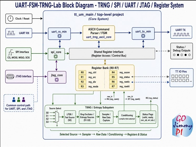
7. Functional Block Diagram
              Tiny Tapeout pins
                    |
                    v
              tt_um_main.v
                    |
        +-----------+------------+
        |                        |
        v                        v
  UART RX/TX path          Optional SPI path
  uart_rx_min.v            spi_slave.v
  uart_tx_min.v                  |
        |                        |
        +-----------+------------+
                    |
                    v
          trng_cfg_ascii_core.v
          ASCII parser + registers
                    |
                    v
            trng_lab_core.v
       LFSR / RO / mixed sampling
                    |
                    v
       status, raw low byte, raw high byte
8. Clock and Reset
| Signal | Active level | Description |
|---|---|---|
clk |
Rising edge | Main synchronous project clock |
rst_n |
Low | Global reset |
On reset, the register bank is initialized as shown below:
| Register | Reset value |
|---|---|
reg_ctrl |
0x00 |
reg_src |
0x00 |
reg_div |
0x10 |
reg_mode |
0x00 |
reg_oscen |
0x01 |
The TRNG lab core internally resets the LFSR to 0x1ACE, clears sample_shift, clears the sample counter, clears status, and clears raw output registers.
9. Tiny Tapeout Pin Map
Dedicated inputs: ui_in[7:0]
| Pin | Direction | Function |
|---|---|---|
ui_in[7:5] |
Input | Reserved / unused |
ui_in[4] |
Input | SPI/JTAG select, 0 = SPI, 1 = JTAG (INPUT Dip Switch SW4 down; when JTAG_ENABLED is defined) |
ui_in[3] |
Input | UART RX |
ui_in[2:0] |
Input | Reserved / unused |
The UART RX input is synchronized through a two-stage synchronizer before it enters the UART receive logic.
Dedicated outputs: uo_out[7:0]
| Pin | Direction | Function |
|---|---|---|
uo_out[0] |
Output | Debug visibility: trng_bit |
uo_out[1] |
Output | Debug visibility: reg_status[0] |
uo_out[2] |
Output | Debug visibility: reg_status[1] |
uo_out[3] |
Output | Debug visibility: reg_status[2] |
uo_out[4] |
Output | UART TX |
uo_out[5] |
Output | reg_rawlo[0] |
uo_out[6] |
Output | reg_rawlo[1] |
uo_out[7] |
Output | reg_rawlo[2] |
Bidirectional IO: uio[7:0] when SPI is enabled
| Pin | Direction | Function |
|---|---|---|
uio[0] |
Input | SPI CS_N |
uio[1] |
Input | SPI MOSI |
uio[2] |
Output | SPI MISO |
uio[3] |
Input | SPI SCK |
uio[7:4] |
Output | reg_rawhi[7:4] debug visibility |
When SPI is enabled, uio_oe is driven as 0xF4, making uio[2] and uio[7:4] outputs while leaving uio[0], uio[1], and uio[3] as inputs.
Bidirectional IO when SPI is disabled
When SPI is not enabled, uio_out[7:0] drives the full reg_rawhi byte and uio_oe is driven as 0xFF.
10. UART Interface
UART settings
| Setting | Value |
|---|---|
| Baud rate | UART_BAUD, default 115200 |
| Data bits | 8 |
| Parity | None |
| Stop bits | 1 |
| Byte order | ASCII command bytes |
| Command terminator | Carriage return, 0x0D |
Line feed, 0x0A, is ignored in command wait states, allowing common CRLF terminal behavior.
UART command summary
| Command | Arguments | Effect | Reply |
|---|---|---|---|
Bxx |
2 hex nibbles, 01..FF |
Stream xx raw binary bytes from reg_rawlo/reg_rawhi alternately, when TRNG_BINARY_STREAM is enabled |
Binary bytes, no OK<CR> |
E0 / E1 |
1 hex nibble | Write reg_ctrl[0], TRNG enable |
OK<CR> |
Sx |
1 hex nibble | Write reg_src[1:0] |
OK<CR> |
Vx |
1 hex nibble | Write reg_ctrl[1], deterministic single-step request |
OK<CR> |
Wx |
1 hex nibble | Write reg_ctrl[2], TRNG reset control |
OK<CR> |
Dxx |
2 hex nibbles | Write reg_div[7:0] |
OK<CR> |
Mxx |
2 hex nibbles | Write reg_mode[7:0] |
OK<CR> |
Oxx |
2 hex nibbles | Write reg_oscen[7:0] |
OK<CR> |
Rn |
n = 0..7 |
Read register n |
Rn=HH<CR> |
V |
None | Version query | Version string + <CR> |
Invalid syntax returns ?<CR>.
UART command examples
V<CR>       -> Version 1.0.5 6/21/2026<CR>
R2<CR>      -> R2=10<CR>
E1<CR>      -> OK<CR>
D10<CR>     -> OK<CR>
S0<CR>      -> OK<CR>
O01<CR>     -> OK<CR>
R6<CR>      -> R6=HH<CR>
R7<CR>      -> R7=HH<CR>
To reconstruct the current 16-bit raw sample from UART register reads:
raw16 = (R7 << 8) | R6
11. SPI Interface
The SPI interface is available when SPI_ENABLED and SPI_REG_ACCESS are enabled.
SPI electrical/protocol settings
| Setting | Value |
|---|---|
| Mode | SPI mode 0 |
| CPOL | 0 |
| CPHA | 0 |
| Bit order | MSB first |
| Chip select | Active low, CS_N |
| Register address width | 3 .. 7 bits (see project_config.v ) |
SPI command byte
| Bit field | Description |
|---|---|
bit[7] |
1 = read, 0 = write |
bit[6:3] |
Ignored |
bit[2:0] |
Register address 0..7 or 0..15 or 0..127 (see project_config.v ) |
SPI read transaction
byte 0: 0x80 | addr
byte 1: dummy byte; returned MISO byte is the register value
For example, reading reg_rawlo at address 6:
TX: 86 00
RX: xx HH
The useful read value is the second received byte.
SPI write transaction
byte 0: addr
byte 1: data byte
Only addresses 0 through 4 are writable. Writes to addresses 5 through 7 are ignored by the register bank.
For example, writing divider register R2 = 0x10:
TX: 02 10
12. Register Map
| Addr | UART read | Name | Access | Reset | Description |
|---|---|---|---|---|---|
| 0 | R0 |
reg_ctrl |
R/W | 0x00 |
Control bits |
| 1 | R1 |
reg_src |
R/W | 0x00 |
Source selection |
| 2 | R2 |
reg_div |
R/W | 0x10 |
Sample divider |
| 3 | R3 |
reg_mode |
R/W | 0x00 |
Mode/debug field |
| 4 | R4 |
reg_oscen |
R/W | 0x01 |
Ring oscillator enable mask |
| 5 | R5 |
reg_status |
Read-only | 0x00 |
Status mirror |
| 6 | R6 |
reg_rawlo |
Read-only | 0x00 |
Raw sample low byte |
| 7 | R7 |
reg_rawhi |
Read-only | 0x00 |
Raw sample high byte |
13. Control Register: reg_ctrl, Address 0
| Bit | Name | Description |
|---|---|---|
| 0 | enable |
Enables periodic sampling when set |
| 1 | step |
Deterministic single-step request. A rising edge creates one sample event |
| 2 | reset |
Resets the TRNG lab core while asserted |
| 7:3 | Reserved | Currently unused |
UART aliases:
| Command | Field |
|---|---|
E0 / E1 |
reg_ctrl[0] |
V0 / V1 |
reg_ctrl[1] |
W0 / W1 |
reg_ctrl[2] |
Note: bare V<CR> is the version query. V0<CR> and V1<CR> are control writes.
14. Source Register: reg_src, Address 1
Only reg_src[1:0] is used.
| Value | Source | Description |
|---|---|---|
0 |
SRC_LFSR |
LFSR bit source, deterministic and repeatable |
1 |
SRC_RO0 |
Sampled ring oscillator 0 source |
2 |
SRC_ROX |
XOR of the ring oscillator raw bits |
3 |
SRC_MIX |
Mixed source using RO XOR, LFSR taps, and sample history |
UART alias: Sx<CR> writes reg_src[1:0].
15. Divider Register: reg_div, Address 2
reg_div controls the periodic sample interval when reg_ctrl[0] is enabled. The internal sample counter increments while enabled. A sample event is generated when:
sample_ctr >= reg_div
A single-step event through reg_ctrl[1] can also generate a sample event without waiting for the periodic divider.
UART alias: Dxx<CR> writes the full divider byte.
16. Mode Register: reg_mode, Address 3
reg_mode is a full 8-bit writable register. In the current TRNG lab core, reg_mode[2:0] is mirrored into reg_status[7:5]. Other bits are reserved for future use.
UART alias: Mxx<CR> writes the full mode byte.
17. Oscillator Enable Register: reg_oscen, Address 4
reg_oscen is an 8-bit enable mask for the ring oscillator instances in real RO builds.
There's a conditional BASIC_RO_SET (not defined) in trng_lab_core.v for RO states 3 .. 17.
The default build contains 7 .. 21 stages:
| Bit | Real RO instance | Stage count |
|---|---|---|
| 0 | u_ro0 |
7 |
| 1 | u_ro1 |
9 |
| 2 | u_ro2 |
11 |
| 3 | u_ro3 |
13 |
| 4 | u_ro4 |
15 |
| 5 | u_ro5 |
17 |
| 6 | u_ro6 |
19 |
| 7 | u_ro7 |
21 |
In FPGA and normal simulation builds, the RO raw bits are derived from LFSR taps instead of real ring oscillators.
UART alias: Oxx<CR> writes the full oscillator enable mask.
18. Status Register: reg_status, Address 5
| Bit field | Description |
|---|---|
bit[0] |
Mirrors TRNG enable |
bit[1] |
Mirrors sample tick condition |
bit[2] |
Indicates at least one oscillator enable bit is set |
bits[4:3] |
Mirrors source selection |
bits[7:5] |
Mirrors reg_mode[2:0] |
reg_status is read-only from the external UART/SPI register interfaces.
19. Raw Output Registers: reg_rawlo and reg_rawhi
The TRNG lab core maintains a 16-bit sample shift register. On each sample event, the selected source bit is shifted into the sample history and the raw output registers are updated.
| Register | Description |
|---|---|
reg_rawlo |
Low byte of the latest raw sample history |
reg_rawhi |
High byte of the latest raw sample history |
The current 16-bit raw sample value is reconstructed as:
raw16 = (reg_rawhi << 8) | reg_rawlo
20. Sampling Behavior
A sample event occurs when either condition is true:
do_sample = (enable && sample_tick) || step_pulse
Where:
sample_tick = sample_ctr >= reg_div
step_pulse  = reg_ctrl[1] && !previous_reg_ctrl_bit_1
On each sample event:
sample_ctris cleared to zero- The 16-bit LFSR advances
- The selected source bit shifts into
sample_shift reg_rawloandreg_rawhiare updated
When enable is deasserted, the sample counter is held at zero. A single-step pulse can still advance one sample.
21. LFSR Details
The deterministic LFSR path is used for repeatable tests and for FPGA/simulation-safe substitute RO signals. On TRNG reset, the LFSR seed is:
0x1ACE
The next LFSR bit is computed as:
lfsr_next_bit = lfsr[15] ^ lfsr[13] ^ lfsr[12] ^ lfsr[10]
The LFSR then shifts as:
lfsr <= {lfsr[14:0], lfsr_next_bit}
This path is deterministic and should not be treated as an entropy source.
22. Ring Oscillator Path
In real ASIC RO builds, the default design instantiates eight odd-length ring oscillators with stage counts from 7 to 21. The oscillator outputs feed the source selection logic through synchronizers.
In FPGA and normal simulation builds, real ring oscillators are not instantiated. Instead, the RO raw signals are mapped to LFSR taps so the rest of the design can be tested safely without combinational oscillator loops.
Supported real RO PDK cell paths in the current source are:
| PDK define | Inverter cell |
|---|---|
PDK_TARGET_SKY130 |
sky130_fd_sc_hd__inv_2 |
PDK_TARGET_GF180 |
gf180mcu_fd_sc_mcu7t5v0__inv_2 |
23. Recommended Bring-Up Sequence
A conservative UART bring-up sequence is:
V<CR>       Read version string
R0<CR>      Confirm control reset value
R1<CR>      Confirm source reset value
R2<CR>      Confirm divider reset value, expected 10
R3<CR>      Confirm mode reset value
R4<CR>      Confirm oscillator enable reset value, expected 01
S0<CR>      Select deterministic LFSR source
D10<CR>     Set divider to 0x10
M00<CR>     Clear mode
O01<CR>     Enable oscillator mask bit 0
E1<CR>      Enable sampling
R6<CR>      Read raw low byte
R7<CR>      Read raw high byte
For deterministic regression testing, use source S0, assert and release reset through W1 and W0, then issue single-step pulses through V1 and V0 as required by the test harness.
24. Known Deterministic Regression Sequence
With the deterministic LFSR path and the established single-step/reset test flow, the known-good 16-bit sample sequence used in current hardware regression is:
sample 01: 0x7F2E
sample 02: 0x9F33
sample 03: 0xFC1C
sample 04: 0x6F03
sample 05: 0x4B7D
sample 06: 0x52C8
sample 07: 0xD6B7
sample 08: 0xEF2A
This sequence is a reproducibility check for the deterministic path. It is not an entropy-quality claim.
25. UART and SPI Concurrency Notes
UART and SPI share the same logical register bank. SPI writes are applied when spi_reg_wr_en is asserted. UART commands also update the same configuration registers.
When using SPI as a passive monitor while UART is active, individual register reads are separate transactions. Reading reg_rawlo and reg_rawhi separately is not atomic, so the two bytes may occasionally come from adjacent sample updates. For exact sample capture, add an atomic snapshot/latch mechanism or temporarily stop sampling before reading both bytes.
26. Limitations
- No cryptographic certification is claimed.
- No built-in conditioner, extractor, or DRBG is provided by this RTL block.
- Raw RO entropy quality must be measured on the actual ASIC implementation.
- FPGA and normal simulation builds do not use real ring oscillators.
- SPI multi-byte reads of raw low/high registers are not atomic.
- UART command parsing is intentionally small and accepts only the documented command forms.
- Register addresses 5 through 7 are read-only through SPI writes and UART write aliases do not target them.
27. Characterization Recommendations
Before using ASIC RO output as a source of entropy, characterize at minimum:
- Raw bit bias for each source selection
- Bit transition rate
- Autocorrelation
- Per-oscillator behavior across voltage and temperature
- Behavior across process corners and multiple chips
- Startup behavior after reset
- Sensitivity to
reg_divandreg_oscen - Health test behavior under stuck oscillator conditions
For security use, add a conditioning function and a health-test strategy appropriate for the target application.
28. Revision History
| Datasheet rev | Date | Notes |
|---|---|---|
| 0.1 | 2026-05-23 | Initial datasheet generated from current TRNG source package |
Example Outputs
IO
| # | Input | Output | Bidirectional |
|---|---|---|---|
| 0 | reserved_in0 | trng_bit | spi_cs_n_jtag_tms |
| 1 | reserved_in1 | status0 | spi_mosi_jtag_tdi |
| 2 | reserved_in2 | status1 | spi_miso_jtag_tdo |
| 3 | uart_rx | status2 | spi_sck_jtag_tck |
| 4 | spi_jtag_sel | uart_tx | rawhi4 |
| 5 | reserved_in5 | rawlo0 | rawhi5 |
| 6 | reserved_in6 | rawlo1 | rawhi6 |
| 7 | reserved_in7 | rawlo2 | rawhi7 |