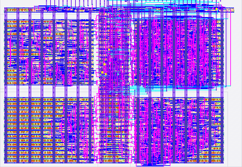
327 Micro tile container
327 : Micro tile container
- Author: Uri Shaked
- Description: Experimental microtile container
- GitHub repository
- Open in 3D viewer
- Clock: 0 Hz
How it works
Combined 4 micro tile sized projects into a single Tiny Tapeout tile.
Selecting the active project
Use uio[1:0] to select the active micro-tile project.
Project 0 - Test
- Repo: https://github.com/TinyTapeout/tt-micro-tiles-experiment
- Author: Uri Shaked
- Description: Micro tiles test module
How it works
The micro tiles test module is a simple module that demonstrates the use of the micro tile interface.
It has two modes of operation:
- Mirroring the input pins to the output pins (when
rst_nis low). - Outputing a counter on the output pins and the bidirectional pins (when
rst_nis high).
The counter is an 8-bit counter that increments on every clock cycle, and resets when rst_n is low.
How to test
- Set
rst_nlow and observe that the input pins (ui_in) are output on the output pins (uo_out). - Set
rst_nhigh and observe that the counter is output on the output pins (uo_out).
Project 1 - Micro Shift Reg ALU
- Repo: https://github.com/MichaelBell/tt-micro-tiles-serial-compute
- Author: Michael Bell
- Description: Micro tiles shift register and 8-bit compute
How it works
A 16-bit shift register that is clocked in from ui_in[0]. The low and high byte can be output on uo_out.
Additionally the result of certain computations of the low and high byte of the shift register can be latched and displayed:
- When ui_in[4] is high the result of ADDing the low and high bytes of the shift regsiter is latched
- When ui_in[5] is high the result of ANDing the low and high bytes of the shift regsiter is latched
How to test
Clock data in on ui_in[0].
ui_in[2:1] select the output, as follows
| ui_in[2:1] | Output |
|---|---|
| 0 | Low byte of shift register |
| 1 | High byte of shift register |
| 2 | Latched ADD result |
| 3 | Latched AND result |
Finally, if rst_n is high the outputs mirror the inputs. Reset is otherwise unused.
Project 2 - PDM CIC Filter
- Repo: https://github.com/gfg-development/tt-micro-tiles-cic
- Author: Gerrit Grutzeck
- Description: Micro tiles CIC filter for PDM signals with a 2 stage filter and a downsampling of 4
How it works
On ui_in[0] the input PDM datastream is received. Then it is processed in a CIC filter with 2 stages and a downsampling factor of 4.
The resulting filtered samples are outputted on uo_out[7:2] and the downsampled clock on uo_out[0]. Furthermore on uo_out[1] the normal clock is available.
How to test
Connect a PDM microphone as follows:
- Clock:
uo_out[1] - Data:
ui_in[0]
Then configure the clock generator of the RP2040 to generate a clock, as needed by the microphone (typically around 2 MHz) and reset the design via rst_n.
After the reset is removed again, the design is up and running, filtering the incoming datastream.
With a connected logic analyzer or the RP2040 the filtered data can now be received on uo_out[7:2], as well as the downsampled clock on uo_out[0].
The downsampled clock can be used to latch the filtered data.
Project 3 - Synchronous FIFO
How it works
A generic synchronous First-In-First-Out (FIFO) buffer. It operates on a single clock domain and allows for buffering of data from an input interface (ui_in) to an output interface (uo_out), while ensuring that data is neither overwritten when full nor read when empty.
Parameters
DATA_WIDTH: The width of the data in bits (default: 6).DEPTH: The depth of the FIFO in terms of the number of entries (default: 3).
Details:
FIFO Depth:
- The default depth is set to 3 for practical reasons for a micro-tile, but this can be modified via the
DEPTHparameter.
FIFO Width:
- The FIFO supports a 6-bit data width, which can also be adjusted via the
DATA_WIDTHparameter.
Reset:
- The
rst_nsignal resets the FIFO, clearing its contents by resetting the write and read pointers (wr_ptrandrd_ptr).
Data Write:
- Data from the
ui_inbus is written to the FIFO when the write enable signal (wr_en) is asserted (bit 6 ofui_in). - The FIFO prevents writing if the buffer is full, indicated by the
o_fullsignal.
Data Read:
- Data is read from the FIFO when the read enable signal (
rd_en) is asserted (bit 7 ofui_in). - The FIFO prevents reading if the buffer is empty, indicated by the
o_emptysignal.
Control Signals:
o_full: Indicates when the FIFO has reached its maximum capacity.o_empty: Indicates when the FIFO has no data to read.
How to test
-
Write Operation:
- Set the
wr_ensignal (ui_in[6]) high and ensureo_fullis low (uo_out[6]). - Apply a 6-bit data value on the lower 6 bits of
ui_in[5:0]untilo_fullis high.
- Set the
-
Read Operation:
- Set the
rd_ensignal (ui_in[7]) high and ensureo_emptyis low (uo_out[7]). - Observe that data is read from the FIFO and appears on the lower 6 bits of
uo_out[5:0]. - Once all the data has been read the
o_emptysignal will go high (uo_out[7]).
- Set the
Inputs and Outputs Table
| Signal | Description |
|---|---|
ui[0] |
FIFO Read Enable |
ui[1] |
FIFO Write Enable |
ui[2] |
FIFO Data Input 1 |
ui[3] |
FIFO Data Input 2 |
ui[4] |
FIFO Data Input 3 |
ui[5] |
FIFO Data Input 4 |
ui[6] |
FIFO Data Input 5 |
ui[7] |
FIFO Data Input 6 |
uo[0] |
FIFO Empty Signal |
uo[1] |
FIFO Full Signal |
uo[2] |
FIFO Data Output 1 |
uo[3] |
FIFO Data Output 2 |
uo[4] |
FIFO Data Output 3 |
uo[5] |
FIFO Data Output 4 |
uo[6] |
FIFO Data Output 5 |
uo[7] |
FIFO Data Output 6 |
IO
| # | Input | Output | Bidirectional |
|---|---|---|---|
| 0 | in[0] | out[0] | sel[0] |
| 1 | in[1] | out[1] | sel[1] |
| 2 | in[2] | out[2] | |
| 3 | in[3] | out[3] | |
| 4 | in[4] | out[4] | |
| 5 | in[5] | out[5] | |
| 6 | in[6] | out[6] | |
| 7 | in[7] | out[7] |