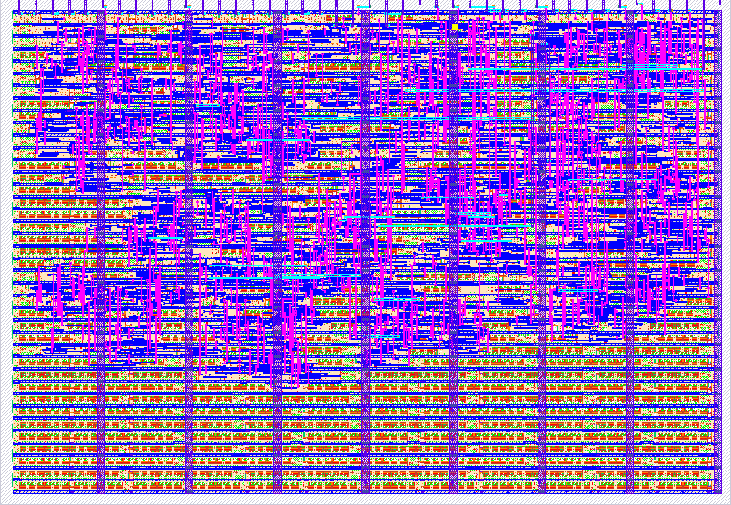
79 Phase Shifted PWM Modulator
79 : Phase Shifted PWM Modulator

- Author: Nelson Salvador & Francisca Donoso
- Description: Phase-Shifted Pulse Width Modulation (PS-PWM) that generates the switching signals for 2 PMOS and 2 NMOS from a duty cycle (d1 and d2)
- GitHub repository
- Open in 3D viewer
- Clock: 1000 Hz
How it works
The Phase Shifted PWM (PS-PWM) system generates phase-shifted PWM signals used for controlling power converters. The main module orchestrates the process by integrating various submodules. It starts by receiving and assigning inputs, then uses a shift register to process serial data, which determines control signals for selecting clock sources and phase-shifted triangular waveforms. These waveforms are generated by dedicated modules for different phases (0, 90, 180, and 270 degrees). The system selects the appropriate phase for two channels and compares these waveforms with input data to produce raw PWM signals. Dead time generators add configurable delays to these signals to prevent transistor cross-conduction. Finally, an output multiplexer and enable control ensure the PWM signals are correctly outputted based on enable signals, producing the desired PS-PWM output.
How to test
1. Initial Setup
- Connect Power Supply:
- Ensure the module is powered correctly.
- Clock Signal:
- Connect a function generator to the
clkinput.
- Connect a function generator to the
- Control Signals:
- Connect switches or signal sources for
rst_n,CLK_SR, anddata_SR.
- Connect switches or signal sources for
- Inputs:
- Connect
ui_inanduio_into signal sources like DIP switches or a microcontroller.
- Connect
2. Reset the Module
- Procedure:
- Set
rst_nto low to reset the module. - Observe the module's outputs to confirm they reset.
- Set
rst_nto high to release the reset.
- Set
3. Shift Data into the Shift Register
- Procedure:
- Set
data_SRto the first bit of your 11-bit data (1or0). - Pulse
CLK_SRhigh, then low to clock in the bit. - Repeat for each bit in your data sequence (e.g.,
11'b00011001101. Sequentially input each bit representing dt[0] to dt[4], SELECTOR_SIGNAL_GENERATOR_1[0], SELECTOR_SIGNAL_GENERATOR_1[1], SELECTOR_SIGNAL_GENERATOR_2[0], SELECTOR_SIGNAL_GENERATOR_2[1], OUTPUT_SELECTOR_EXTERNAL[0], and OUTPUT_SELECTOR_EXTERNAL[1] into the data_SR input. For each bit, you set data_SR to the corresponding value (1 or 0) and toggle CLK_SR high, then low, to clock in the bit. This sequential shifting ensures that each data_out corresponds to the specified comment name within the Shift_Register module.).
- Set
4. Configure ui_in and uio_in (example, 20% duty cycle)
- Procedure:
- Set
ui_into11010000to setd1 = 13(d1 and d2 are 6 bit length, so 13/64 is about 20%). - Set
uio_in[3:0]to1101to set part ofd2 = 13.
- Set
5. Monitor Outputs
- Procedure:
- Use an oscilloscope or logic analyzer to check
uo_outsignals. - Verify the PWM signals on
uo_out[0](PMOS1),uo_out[1](NMOS2),uo_out[2](PMOS2),uo_out[3](NMOS1), and the clock signal onuo_out[4]. - Confirm the PWMs duty cycle matches the expected 20%.
- Use an oscilloscope or logic analyzer to check
External hardware
There is no need of external hardware.
IO
| # | Input | Output | Bidirectional |
|---|---|---|---|
| 0 | d1[0] | PMOS1 | d2[2] |
| 1 | d1[1] | NMOS2 | d2[3] |
| 2 | d1[2] | PMOS2 | d2[4] |
| 3 | d1[3] | NMOS1 | d2[5] |
| 4 | d1[4] | clk_in | CLK_SR |
| 5 | d1[5] | Data_SR | |
| 6 | d2[0] | CLK_EXT | |
| 7 | d2[1] |