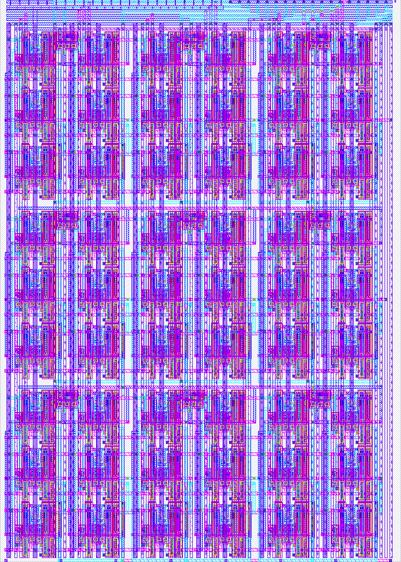
482 Field Programmable Resistor Network
482 : Field Programmable Resistor Network

- Author: htfab
- Description: A few resistors and switches wired up in a matrix pattern.
- GitHub repository
- Open in 3D viewer
- Clock: 0 Hz
- Feedback: ✅ 2
How it works
A few resistors and switches are wired up in a matrix pattern. Switches are implemented as pass gates controlled by latches that keep the configuration. The network can be used as a makeshift DAC by controlling the "bitstream".
Matrix cells can be selected using the H_GATE_i and V_GATE_j inputs:
H_GATE_0=uio_in[5]H_GATE_1=uio_in[2]H_GATE_2=ui_in[1]V_GATE_0=uio_in[6]V_GATE_1=uio_in[3]V_GATE_2=uio_in[0]
When the inputs H_GATE_i and V_GATE_j are on, the latches in the
cell ij become transparent and configure the pass gates as follows:
HR_ij←HD_RES=ui_in[4]HS_ij←HD_SHORT=ui_in[3]HL_ij←HD_LINE=ui_in[2]VR_ij←VD_RES=ui_in[7]VS_ij←VD_SHORT=ui_in[6]VL_ij←VD_LINE=ui_in[5]
Once H_GATE_i or V_GATE_j is off again, the latches close and the
pass gates keep their configuration. Thus a new cell with different
i or j can be configured using the same inputs.
How to test
After the network is configured as above, manipulate the digital inputs
H_INPUT_i and V_INPUT_j to apply 0 V or 1.8 V at the respective nodes
of the network:
HI_0←H_INPUT_0=ui_in[0]HI_1←H_INPUT_1=rst_nHI_2←H_INPUT_2=clkVI_0←V_INPUT_0=uio_in[7]VI_1←V_INPUT_1=uio_in[4]VI_2←V_INPUT_2=uio_in[1]
The voltage can be measured externally at the analog pin AP = ua[0].
External hardware
Multimeter (or microcontroller with ADC) to measure the output voltage.
IO
| # | Input | Output | Bidirectional |
|---|---|---|---|
| 0 | `H_INPUT_0` | `V_GATE_2` | |
| 1 | `H_GATE_2` | `V_INPUT_2` | |
| 2 | `HD_LINE` | `H_GATE_1` | |
| 3 | `HD_SHORT` | `V_GATE_1` | |
| 4 | `HD_RES` | `V_INPUT_1` | |
| 5 | `VD_LINE` | `H_GATE_0` | |
| 6 | `VD_SHORT` | `V_GATE_0` | |
| 7 | `VD_RES` | `V_INPUT_0` |
Analog pins
ua | PCB Pin | Internal index | Description |
|---|---|---|---|
| 0 | A0 | 0 | `ANALOG_PIN` |
User feedback
- mattvenn: Tested the R2R DAC mode, and it worked as expected. Need to cut the 10k pulldown resistor first.
- htfab👑: Tested on the Z2A analog call. Both of the bring-up scripts in the repo work after cutting the jumper next to "A0" on the breakout board, thus disconnecting a 10k resistor to ground present on the demoboard (thanks Sylvain for the suggestion). The resistors in the design are 50k, so without cutting the jumper you will get 10% to 15% of the expected voltage on the "A0" pin but you should still be able to see the design working.