204 The James Retro Byte 8 computer
204 : The James Retro Byte 8 computer

- Author: James Ridey
- Description: A 8bit microprocessor built from the ground up (nand2tetris)
- GitHub repository
- Open in 3D viewer
- Clock: 0 Hz
- Feedback: ✅ 1
Overview
This project is an 8-bit computer I originally designed in Logisim Evolution, which I am now porting to TinyTapeout for manufacturing. Below is the computer’s general architecture as shown in Logisim Evolution; however, certain modifications were made to ensure compatibility with VHDL and TinyTapeout.
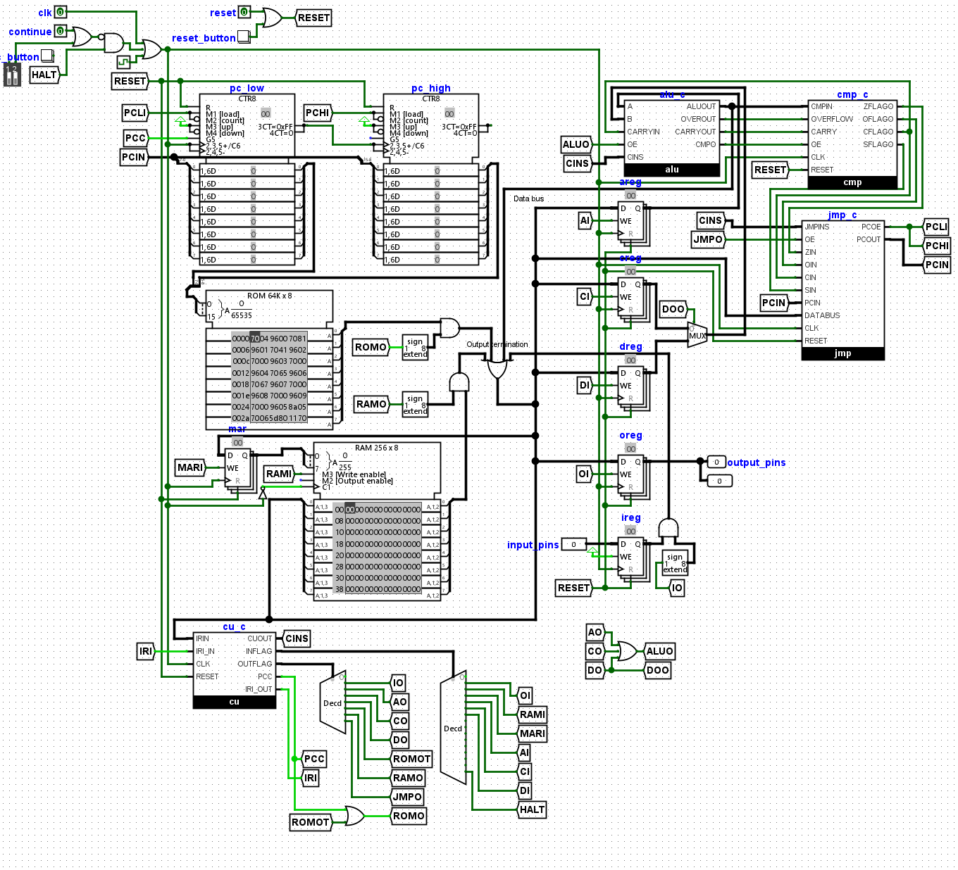
The primary change includes the addition of a B register, alongside adjustments to enable ROM and RAM communication via SPI. Detailed information on these modifications is provided below.
The computer supports the following operations:
Register Operations
The computer features four main registers: a, b, c, and d. It supports:
- Moving (
mov) data between all registers. - Comparing (
cmp) values between registers, or between a register and a constant (0, 1, -1, or 255). - Jumping (
jmp) to labels and performing conditional jumps (=,!=,<,<=,>,>=) and relative jumps.
ALU Operations
The ALU (Arithmetic Logic Unit) offers the following operations:
- Bitwise NOT (
~) and negation (-). - Increment (
+1) and decrement (-1). - Addition (
+) and subtraction (-). - Multiplication (
*) and division (/). - Bitwise AND (
&) and OR (|). - Signed mode operations and a carry flag for extended 8-bit addition/subtraction.
Memory and I/O
- Load data from ROM into a register.
- Load data from RAM into a register.
- Save data from a register to RAM.
- Read from the input (
in) port. - Write to the output (
out) port.
Testing the Computer
The computer doesn't have any start signal and will begin read from the SPI ROM as soon as the clock signal (clk) starts ticking.
For examples of programs and a basic assembler, please see this repository (https://github.com/AeroX2/tt06-jrb8-computer/).
Clone the repository and use the assembler with the following command:
python3 ./example_programs/assembler.py
A file dialog will open, allowing you to select a *.j file.
Sample Program: 8-bit Fibonacci Sequence
Below is a simple 8-bit Fibonacci program in the custom J format (fibonacci.j):
:start
load rom a 1
load rom b 0
:repeat
// Store the previous in c register
mov a c
// a = a + b
opp a+b
// This also corresponds to the carry flag being set
// So jump to start if a+b has overflowed
jmp < start
// Output the value to the output pins
out a
// Restore the previous value in b register
mov c b
jmp repeat
This program, when assembled, translates to the following hexadecimal format:
d0 01 d1 00 02 6c 33 00 00 f4 08 36 00 04
For a comprehensive guide on assembler instructions and their corresponding hex codes, refer to this document (https://docs.google.com/document/d/1ZVZw_Kt-KQHER0Wr5ty7JpUEeox_284Mih4rwE16FVM/edit?usp=sharing).
You can also look at roms/cu_flags.csv in the tt06-jrb8-computer repository
The input register or the i register is mapped to ui_in
The output register or the o register is mapped to uo_out
Memory Mapping
To load data into the ROM, place it at offset 0. The address space is divided as follows:
- ROM (Program Data): 0x0000 to 0xFFFF
- RAM: 0x10000 to 0x1FFFF
RAM Addressing
RAM addressing is handled through two registers:
mpageRegister: Controls0x1**00marRegister: Controls0x100**
External Hardware Requirements
External SPI storage is required for this computer, with mappings compatible with spi-ram-emu (https://github.com/MichaelBell/spi-ram-emu/). The following uio mappings are used:
uio[0]: "cs rom"
uio[1]: "mosi"
uio[2]: "miso"
uio[3]: "sck"
IO
| # | Input | Output | Bidirectional |
|---|---|---|---|
| 0 | input bit 0 | output bit 0 | cs rom |
| 1 | input bit 1 | output bit 1 | mosi |
| 2 | input bit 2 | output bit 2 | miso |
| 3 | input bit 3 | output bit 3 | sck |
| 4 | input bit 4 | output bit 4 | cs ram |
| 5 | input bit 5 | output bit 5 | |
| 6 | input bit 6 | output bit 6 | |
| 7 | input bit 7 | output bit 7 | 24 addressing bit mode |
User feedback
- AeroX2👑: Tested a simple repeating output program and it works! Next steps: - Get spi-ram-emu working - Test a more complicated program - Test an even more complicated program! Link for more details